Other Parts Discussed in Thread: AM62D-Q1, AM62L, AM62P, AM62A3, AM6422, AM623, AM2431, , AUDIO-AM62D-EVM, SN74LVC1G17, SYSCONFIG, AM2432, DRA829J, AM62A7-Q1, AM6442, AM62A3-Q1
Tool/software:
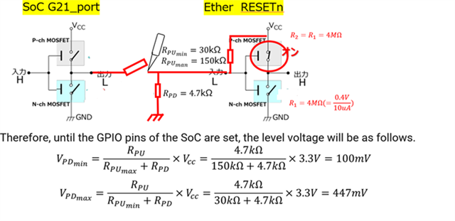
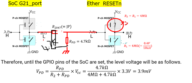
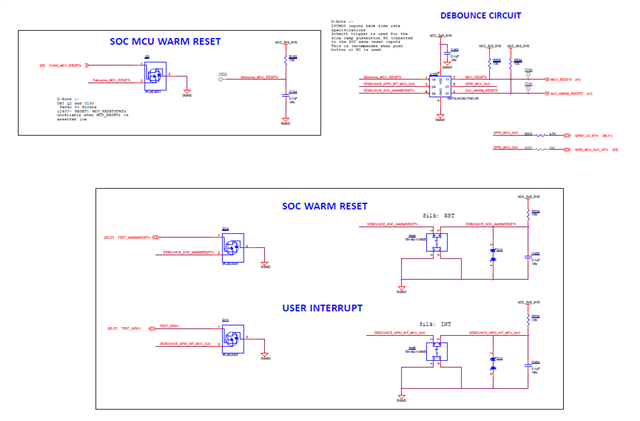
Hi TI Experts,
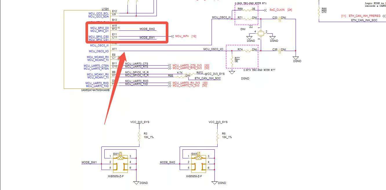
Do you have recommendations on using the GPIOs - Configuration, Slew rate, Current drive, Buffer type, and interfacing to external signals