This thread has been locked.

If you have a related question, please click the "Ask a related question" button in the top right corner. The newly created question will be automatically linked to this question.

AM6442: Using an event to trigger a DMA SPI Read

Part Number: AM6442
Other Parts Discussed in Thread: ADS127L18, SYSCONFIG, TMDS64EVM

Tool/software:

Dear TI experts,

We have the following hardware configuration:

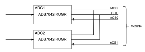
The two ADCs are attached to McSPI4 in multi-controller mode on an AM6442 SoC and are to be used on the R5F side. The requirements are as follows:

  • 128 KSPS readout rate
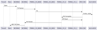
  • Sequential readout, first ADC1 and then ADC2. We have to be able to distinguish the data source, i.e., if the sample comes from ADC1 or ADC2
  • Stable readout frequency - max. jitter 10ns
  • Interrupt every 32 samples

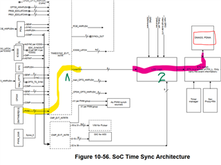
We already have another ADC, attached to the SoC (8-channel ADS127L18), which acts as an SPI master and generates nCS and clock for 2 McSPI in peripheral mode. This ADC is being read out through PKTDMA+PDMA, being triggered on an McSPI RX.

Our intention was to use either the nCS, generated from the ADS127L18 (internally, as an internal trigger, or externally, as a GPIO interrupt), or a timer to trigger a second DMA, which has to read both ADCs sequentially.

Please note that a timer interrupt is not an option here, as it will cause a significant amount of jitter, leading to distortion in the digitized signal. We need a stable readout frequency.

We have the following questions:

  1. Apparently, PKTDMA cannot be triggered from an arbitrary trigger source; it has to be a packet/event generated from a peripheral. That means that we have to use BCDMA, correct? Is the usage of BCDMA compatible with PDMA for McSPI?
  2. What will be the way to configure the BCDMA to use an internal signal, such as RX Complete from another McSPI (for example, McSPI 3), which signal is used to trigger the DMA transfer from another McSPI?
  3. BCDMA has to be configured to read both ADCs, ADC1 and ADC2 sequentially, since they share the same McSPI. In theory, those are 2 separate SPI channels, but can the DMA be chained in such a way that:
    • An external event (ADS127L18 nCS, GPIO interrupt, or a timer) triggers the readout of ADC1
    • When completed, McSPI TX Complete of ADC1 triggers the readout of ADC2
  4. Do we probably need more than one BCDMA channel to achieve the above?

Thank you!

  • Hello Angel,

    I am looking at your queries and you may get reply on Monday .

    Regards,

    Anil.

  • Now that I have a better idea of what should or could be done, I have drawn a sequence diagram illustrating how I envision the process:

    The above is repeated twice, for McSPI4-CH0 and McSPI4-CH1. The timers, delivering the start trigger, must be configured to work with an offset of at least 1us, since that would be the minimum time to complete the ADC Read (16 clocks@16 Mhz).

    Since it doesn't seem possible to trigger the BCDMA transfer from the event I originally intended (PDMA Transfer Complete or McSPI Peripheral RX Complete), I would like to explore triggering it from an internal DMTimer. According to a related post, this should be feasible, though with an IEP unit in the PRU. Following the same logic, the path from a DMTimer PWM Output could also be utilized, according to the TRM.

    From my understanding, this approach should be possible. If I am correctly interpreting the TRM, the events from Timer0 to Timer3 should be usable to trigger the BCDMA.

    Additionally, for the BCDMA channels, it appears that separate RX and TX channels should be used to connect to the PDMAs of the McSPI. Is that correct?

    I still have the following open questions:

    1. Is the above observation correct at all?
    2. How can the event routing from the corresponding timers (Timer0 to Timer3) to the L2G be configured?
    3. How should the BCDMA Tx channels be configured to be triggered by those timers?
    4. Is it possible for one BCDMA Tx channel (McSPI4-Ch1) to be triggered by the rising edge of a PWM output, while another BCDMA Tx channel (McSPI4-Ch1) is triggered by the falling edge of the same output?

    Thanks and regards!

  • Hi Anil,

    do you already have any ideas? Our hardware design is dependent on the feasibility of the concept and we only have a couple of days left to make a decision.

    Thanks!

  • Hello Angel,

    I can give suggestions by today and need to spend some time to analysis on your requirements and solution .

    Regards,

    Anil.

  • Hello Angel,

    Summary of Setup :

    • Two SPI ADCs connected to McSPI4, configured in multi-controller mode.

    • A separate ADS127L18 (master ADC) generates SCLK and nCS for the two peripheral SPI ADCs.

    • Readout rate: 128 kSPS

    • Read Order: Sequential read: ADC1 → ADC2

    • Interrupt: Every 32 samplesDesign :

    Method : 

    Use BCDMA + PDMA on R5F. Since the McSPI is in peripheral mode, you can configure BCDMA + PDMA. 

    Configure McSPI4 in multi-controller mode

    • Use chip select lines (nCS0 and nCS1) separately for ADC1 and ADC2.

    • ADS127L18 must toggle nCS for ADC1 and ADC2 in a defined, repeatable sequence.

    • This sequence will be used to map the source of data.

    • You can route the nCS signals as external trigger inputs to BCDMA DMA channels, if you want back-to-back transfer from both ADCs.

    • Configure two McSPI RX DMA channels, one for ADC1 and one for ADC2.

    • Ensure that each DMA channel is triggered by its respective nCS and SPI RX event.

    • DMA Interrupt every 32 Samples (Set DMA transfer size = 32 samples per ADC. )

    Trigger Mechanism : 

    ADS127L18 drives SCLK and toggles nCS1 → ADC1 responds → SPI RX triggers DMA1.

    Immediately after,

    ADS127L18 toggles nCS2 → ADC2 responds → SPI RX triggers DMA2.

    Challenges : 

    The MCSPI is used with DMA in the PKTDMA manner and this PKTDMA is not supposed to load infinite times TR, and it is not possible to trigger the DMA event continuously. 

    Here, you need to go with BCDMA, this is possible and in MCU+SDK we don't support MCSPI with the BCDMA channel.

    If we configure MCSPI with BCDMA channels , your requirement can be implemented with the DMA auto triggers .

    And, the DMA is triggered based on the GPIO input, which is possible with BCDMA.

    You can look at the FAQ below on how to trigger DMA from the GPIO input.

    https://e2e.ti.com/support/processors-group/processors/f/processors-forum/1378150/faq-how-to-trigger-dma-with-the-help-of-gpio-on-am64x-am243-and-am62x-devices

    Regards,

    Anil.

  • Hi Anil,

    Thanks for your comprehensive reply. However, I don’t think it fully addresses my use case. Let me explain again:

    I need a BCDMA/PDMA configuration that meets the following criteria:

    1. We have decided to forgo triggering from the main ADC for now. Instead, our entire chain will be triggered by the DMTIMER0 in PWM mode, which delivers a pulse every 7.8125 µs (128 KHz) with a duration of 500 ns.
    2. This trigger should initiate a BCDMA write transfer to MCSPI4, CH0.
    3. Upon completion of (2), another PKTDMA/PDMA read channel on MCSPI4, CH0 should automatically be triggered via a DMA read request.
    4. Simultaneously, the completion of (2) should trigger another BCDMA write transfer on a separate channel to MCSPI4, CH1.
    5. This, in turn, should automatically trigger another PKTDMA/PDMA read channel on MCSPI4, CH1 via a DMA read request.
    6. After 32 SPI4-CH1 reads, an interrupt will be generated, at which point the gathered data will be processed.

    We already know how to implement points (3) and (5). I believe I have successfully triggered (2) from (1). My main question now is: How can (4) be triggered by (2)?

    To summarize, we are working with four DMA channels:

    • 2 BCDMA-PDMA channels
    • 2 PKTDMA-PDMA channels

  • Hello Angel,

    Can you please confirm how many bytes are written on the SPI register with the BCDMA - PDMA SPI ?

    Can you please share a snippet of how you configured this BCDMA -PDMA SPI ? 

    With the above attached FAQ, you can  AUTO trigger the DMA from the Timer PWM.

    Next, you need to chain the second and fourth points and this is possible with DMA chaining .

    The DMA changing is only possible on the BCDMA channels.

    Please look at the example below.

    C:\ti\mcu_plus_sdk_am64x_10_01_00_32\examples\drivers\udma\udma_chaining\am64x-evm

    Regards,

    Anil.

  • Hi Anil, 

    We are trying to write 16-bit to the SPI, so it can also output 16 bit to the ADC.

    Please find some code segments below, however I am absoletly not sure if that is the correct configuration. 

    std::error_code TxEngine::Init() 
    {
        //The engine has the following setup:
        //  1. BCDMA Ch0 is coupled with PDMA McSPI4-0 TX. BCDMA Ch1 is coupled with PDMA McSPI4-1 TX  
        //  2. PKDMA Ch0 is coupled with PDMA McSPI4-0 RX, PKDMA Ch1 is coupled with PDMA McSPI4-1 RX
        //  3. DMA Ch0 is triggered from PWM of Timer0 each 7.8125us (in this case) and that triggers an McSPI write of 16 bytes to Aux SPI (TX)
        //      - The trigger signal (Timer) gets reseted (How???)
        //  4. When the TX transfer above is completed, BCDMA Ch1 is triggered and performs a  McSPI4-1 Write (TX)
        //      - At the same time, PKDMA Ch0 is triggered and reads a word from the McSPI4-0 (RX)
        //  5. When the TX transfer from (4) is completed,  PKDMA Ch1 is triggered and reads a word from the McSPI4-1 (RX)
        //  6. When (5) completes, the BCDMA Ch0 waits for the next trigger (Timer)
        //  7. When PKDMA Ch0 & Ch1 gather 32 samples, they deliver an interrupt for the application
        //      - in the interrupt routine, the processd HPDs is removed from the FQ queue and added again at the back.
        //        This ensures continuous transfer of data  
    
        //Configure BCDMA Ch0
        Udma_ChPrms chParams;
        UdmaChPrms_init(&chParams, UDMA_CH_TYPE_PDMA_TX);
        chParams.fqRingPrms.ringMem     = m_udmaCh0RingMem;
        chParams.fqRingPrms.ringMemSize = sizeof(m_udmaCh0RingMem);
        chParams.fqRingPrms.elemCnt = m_UdmaCh0TrCount;
        chParams.peerChNum = UDMA_PDMA_CH_MAIN1_MCSPI4_CH0_TX;
    
        // Open channel for TX
        int32_t retVal = UDMA_SOK;
        retVal = Udma_chOpen(m_udmaHandleBc, m_udmaCh0TxHandle, UDMA_CH_TYPE_PDMA_TX, &chParams);
        if (retVal != UDMA_SOK) {
            return std::make_error_code(TxEngine_ErrorCode::DMAChOpenError);
        }
    
        // Config TX channel
        Udma_ChTxPrms txPrms;
        UdmaChTxPrms_init(&txPrms, UDMA_CH_TYPE_PDMA_TX);
        retVal += Udma_chConfigTx(m_udmaCh0TxHandle, &txPrms);
        if (retVal != UDMA_SOK) {
            return std::make_error_code(TxEngine_ErrorCode::DMAChInitError);
        }
    
        //Configure events
        uint32_t globalEvent0 = Udma_chGetTriggerEvent(m_udmaCh0TxHandle, CSL_UDMAP_TR_FLAGS_TRIGGER_GLOBAL0);
        //Maps Timer0 PWM to the output of the Interrupt Router
        configureRouter(Config::Aux::PulseRoutingDeviceId, Config::Aux::PulseRoutingSourceIdLocal, Config::Aux::PulseRoutingTargetIdLocal);
        //Configure the L2G mapping
        configureIntaggrL2G(Config::Aux::PulseRoutingL2GId, globalEvent0);
    
        //Config the PDMA peer Channel on the McSPI side
        Udma_ChPdmaPrms pdmaPrms;
    
        UdmaChPdmaPrms_init(&pdmaPrms);
        pdmaPrms.elemSize = UDMA_PDMA_ES_16BITS;
        pdmaPrms.elemCnt = 1U;
        pdmaPrms.fifoCnt = 1U;
    
        retVal = Udma_chConfigPdma(m_udmaCh0TxHandle, &pdmaPrms);
        if (retVal != UDMA_SOK) {
            return std::make_error_code(TxEngine_ErrorCode::PDMAConfigureError);
        }
    
        retVal += Udma_chEnable(m_udmaCh0TxHandle);
        DebugP_assert(UDMA_SOK == retVal);
    
        //Submit TRPD to the TX channel
        uint64_t trpdMemPhysicalAddr = (uint64_t)Udma_defaultVirtToPhyFxn(m_udmaCh0TrMem, 0U, NULL);
        retVal = Udma_ringQueueRaw(Udma_chGetFqRingHandle(m_udmaCh0TxHandle), trpdMemPhysicalAddr);
        if (retVal != UDMA_SOK) {
            return std::make_error_code(TxEngine_ErrorCode::DMADescriptorEnqueue);
        }
    
        m_init = true;
    
        return std::error_code();
    }

    Below a summary of the member variables:

        // For each entry in the ring, 64-bit addr
        uint8_t m_Mcspi1UdmaRxRingMemCh0[UDMA_ALIGN_SIZE(m_trCount * sizeof(uint64_t))] __attribute__((aligned(UDMA_CACHELINE_ALIGNMENT)));
        // For each entry in the HDP Memory, a CSL_UdmapCppi5HMPD structure
        uint8_t m_udmaRxHpdMem[UDMA_ALIGN_SIZE(m_trCount * (sizeof(CSL_UdmapCppi5HMPD)))] __attribute__((aligned(UDMA_CACHELINE_ALIGNMENT)));
    
        // UDMA handles
        Udma_DrvHandle m_udmaHandleBc;
    
        //BCDMA Ch0
        static constexpr uint8_t m_UdmaCh0TrCount = Config::Aux::Bcdma0RingElementCount;
        Udma_ChObject m_udmaCh0TxObject;
        Udma_ChHandle m_udmaCh0TxHandle;
        Udma_EventObject m_ch0TxEventObject;
        //Ring memory, where the TRs will be queued
        uint8_t m_udmaCh0RingMem[UDMA_ALIGN_SIZE(m_UdmaCh0TrCount*8U)] __attribute__((aligned(UDMA_CACHELINE_ALIGNMENT)));
        //Memory for the TRs themselves
        uint8_t m_udmaCh0TrMem[UDMA_GET_TRPD_TR15_SIZE(m_UdmaCh0TrCount)] __attribute__((aligned(UDMA_CACHELINE_ALIGNMENT)));
        // Dummy data to be sent to the ADC
        const std::array<uint16_t, 1> m_txData = {0xDEAD}; 
    
        //McSPI specifics
        MCSPILLD_Handle m_spiIf;

    Functions and constants, concerning the mapping of events:

    //Interrupt & L2G mapping
    //We use timer PWM events, which are router trough the Timesync Router
    const uint16_t PulseRoutingDeviceId = TISCI_DEV_TIMESYNC_EVENT_INTROUTER0;  
    //Timer0 has PWM event id 0. Consult TRM 9.5.2/Table 9-73
    const uint16_t PulseRoutingSourceIdLocal = 0;
    const uint16_t PulseRoutingTargetIdLocal = 0;
    //The above PWM event local event will be mapped to bit 0 of the L2G inputs.
    //Consult TRM 11.2.1.2.5
    const uint16_t PulseRoutingL2GId = CSLR_DMASS0_INTAGGR_0_INTAGGR_LEVI_PEND_TIMESYNC_EVENT_INTROUTER0_OUTL_0 + PulseRoutingTargetIdLocal;
    //TX Engine 0 sizes
    const uint8_t Bcdma0RingElementCount = 1;
    
    
    void TxEngine::configureRouter(uint16_t device_id, uint16_t src_index, uint16_t dst_index) {
        int32_t status;
        struct tisci_msg_rm_irq_set_req rmIrqReq;
        struct tisci_msg_rm_irq_set_resp rmIrqResp;
    
        rmIrqReq.valid_params = TISCI_MSG_VALUE_RM_DST_ID_VALID | TISCI_MSG_VALUE_RM_DST_HOST_IRQ_VALID;
        rmIrqReq.src_id = device_id;
        rmIrqReq.dst_id = device_id;
        rmIrqReq.src_index = src_index;
        rmIrqReq.dst_host_irq = dst_index;
        rmIrqReq.secondary_host = TISCI_MSG_VALUE_RM_UNUSED_SECONDARY_HOST;
        status = Sciclient_rmIrqSetRaw(&rmIrqReq, &rmIrqResp, SystemP_WAIT_FOREVER);
    
        if (status != SystemP_SUCCESS) {
            DebugP_log("[Error] Sciclient_rmIrqSetRaw() returned %d.\r\n", status);
            DebugP_log("rmIrqReq.src_id = %d, ", rmIrqReq.src_id);
            DebugP_log("rmIrqReq.src_index = %d, ", rmIrqReq.src_index);
            DebugP_log("dst_host_irq = %d.\r\n", rmIrqReq.dst_host_irq);
        }
    }
    
    void TxEngine::configureIntaggrL2G(uint32_t localEvent, uint32_t globalEvent) {
        uint32_t eventRegOffset = CSL_DMASS0_INTAGGR_L2G_BASE + (localEvent * 0x20U);
        CSL_REG32_WR(eventRegOffset, (1U << 31U) | (globalEvent & 0xFFFFU));
    }

    What I am also unsure is, how to configure the TRs, so that the transfer is repeated on each PWM pulse, so let me post the TR configuration:

    void TxEngine::udmaTxTrInit(uint8_t* pTrMem, uint32_t cqRingNum, const void* srcBuf, uint32_t length)
    {
        //One TRPD (Transfer Packet Descriptor) can have multiple TRs (Transfer Request)
        //Make TRPD with TR15 TR type, size is 1 TR
        UdmaUtils_makeTrpdTr15(pTrMem, 1U, cqRingNum);
        //Set infinte reload count
        CSL_udmapCppi5TrSetReload((CSL_UdmapCppi5TRPD *)pTrMem, 0x1FFU, 0U);
    
        //Get a pointer to the firs t TR in the TRPD and set the TR parameters
        CSL_UdmapTR15* pTr = UdmaUtils_getTrpdTr15Pointer(pTrMem, 0U);
        pTr->flags    = CSL_FMK(UDMAP_TR_FLAGS_TYPE, CSL_UDMAP_TR_FLAGS_TYPE_1D_DATA_MOVE);
        pTr->flags   |= CSL_FMK(UDMAP_TR_FLAGS_STATIC, 0U);
        pTr->flags   |= CSL_FMK(UDMAP_TR_FLAGS_EOL, CSL_UDMAP_TR_FLAGS_EOL_MATCH_SOL_EOL);
        pTr->flags   |= CSL_FMK(UDMAP_TR_FLAGS_EVENT_SIZE, CSL_UDMAP_TR_FLAGS_EVENT_SIZE_COMPLETION);
        pTr->flags   |= CSL_FMK(UDMAP_TR_FLAGS_TRIGGER0, CSL_UDMAP_TR_FLAGS_TRIGGER_GLOBAL0);
        pTr->flags   |= CSL_FMK(UDMAP_TR_FLAGS_TRIGGER0_TYPE, CSL_UDMAP_TR_FLAGS_TRIGGER_TYPE_ICNT1_DEC);
        pTr->flags   |= CSL_FMK(UDMAP_TR_FLAGS_TRIGGER1, CSL_UDMAP_TR_FLAGS_TRIGGER_NONE);
        pTr->flags   |= CSL_FMK(UDMAP_TR_FLAGS_TRIGGER1_TYPE, CSL_UDMAP_TR_FLAGS_TRIGGER_TYPE_ALL);
        pTr->flags   |= CSL_FMK(UDMAP_TR_FLAGS_CMD_ID, 0x25U);  /* This will come back in TR response */
        pTr->flags   |= CSL_FMK(UDMAP_TR_FLAGS_SA_INDIRECT, 0U);
        pTr->flags   |= CSL_FMK(UDMAP_TR_FLAGS_DA_INDIRECT, 0U);
        pTr->flags   |= CSL_FMK(UDMAP_TR_FLAGS_EOP, 1U);
    
        pTr->icnt0    = length;
        pTr->icnt1    = 1U;
        pTr->icnt2    = 1U;
        pTr->icnt3    = 1U;
        pTr->dim1     = pTr->icnt0;
        pTr->dim2     = 0U;
        pTr->dim3     = 0U;
        pTr->addr     = (uint64_t) Udma_defaultVirtToPhyFxn(srcBuf, 0U, NULL);
        pTr->fmtflags = 0x00000000U;
    
        pTr->dicnt0   = 0;
        pTr->dicnt1   = 0;
        pTr->dicnt2   = 0;
        pTr->dicnt3   = 1U;
        pTr->ddim1    = pTr->dicnt0;
        pTr->ddim2    = 0U;
        pTr->ddim3    = 0U;
    
        //Perform cache writeback for 1 TR 
        CacheP_wb(pTrMem, UDMA_GET_TRPD_TR15_SIZE(1), CacheP_TYPE_ALLD);
    
        return;
    }

    About the chaining: yes, I am aware of that example and that is a great news, that it is also possible for our use case. However, I first want to have a stable solution, which repeats the transfers over one channel, then make the next step and chain the next channel transfer.

    Thanks and regards!

  • Hello Angel,

    I need the code snippet of the BCDMA  - PDMA TR descriptor .

    Regards,

    Anil.

  • What I am also unsure is, how to configure the TRs, so that the transfer is repeated on each PWM pulse, so let me post the TR configuration:

    Here I can help you with how to do that ... Already we have the example of triggering the DMA based on the gPIO and here we need to change the input to Timer PWM, and it is doable. 

    But, you have already confirmed that the BCDMA - PDMA part is working.

    So, I am curious about how you configured this TR descriptor  ?

    Simply taking the memcpy TRPD, in this TR , passing the source address of the SPI and configuring the DMA size is 2 bytes ?

    Or taking the HPD and configuring it the DMA length and other parameters.

    Because if you go with the first method, memory TRPD does not support triggering 16-bit data and at least the DMA needs a minimum size to transfer data.

    I remember mostly this minimum value is 64 bytes.

    If you go with the second method, HPD, then you will be able to transfer minimum bytes also.

    I am curious about how you configured the BCDMA - SPI TR descriptor .

    Memcpy Descriptor : 

    HPD descriptor : 

    Regards,

    Anil.

  • Hi Anil,

    I'm starting to feel that I am completely wrong with what I’m doing here. The very first thing I’m trying to achieve is transmitting a 16-bit value to the McSPI interface in a periodic manner (every 7.8125 µs).

    Could you confirm whether the following sequence is correct?

    0) This should be achievable by coupling a BCDMA with a PDMA peer, connected to McSPI4, Ch0.

    1) Initialize and open a BCDMA channel of type UDMA_CH_TYPE_PDMA_TX.

        //Configure BCDMA Ch0
        Udma_ChPrms chParams;
        UdmaChPrms_init(&chParams, UDMA_CH_TYPE_PDMA_TX);
        chParams.fqRingPrms.ringMem     = m_udmaCh0RingMem;
        chParams.fqRingPrms.ringMemSize = sizeof(m_udmaCh0RingMem);
        chParams.fqRingPrms.elemCnt = m_UdmaCh0TrCount;
        chParams.peerChNum = UDMA_PDMA_CH_MAIN1_MCSPI4_CH0_TX;
    
        // Open channel for TX
        int32_t retVal = UDMA_SOK;
        retVal = Udma_chOpen(m_udmaHandleBc, m_udmaCh0TxHandle, UDMA_CH_TYPE_PDMA_TX, &chParams);
        if (retVal != UDMA_SOK) {
            return std::make_error_code(TxEngine_ErrorCode::DMAChOpenError);
        }
    
        // Config TX channel
        Udma_ChTxPrms txPrms;
        UdmaChTxPrms_init(&txPrms, UDMA_CH_TYPE_PDMA_TX);
        retVal += Udma_chConfigTx(m_udmaCh0TxHandle, &txPrms);
        if (retVal != UDMA_SOK) {
            return std::make_error_code(TxEngine_ErrorCode::DMAChInitError);
        }
    

    2) Map the events from DMTIMER0 to the initialized BCDMA channel so that the timer periodically triggers the DMA transfer. This involves:

        //Configure events
        uint32_t globalEvent0 = Udma_chGetTriggerEvent(m_udmaCh0TxHandle, CSL_UDMAP_TR_FLAGS_TRIGGER_GLOBAL0);
        //Maps Timer0 PWM to the output of the Interrupt Router
        configureRouter(Config::Aux::PulseRoutingDeviceId, Config::Aux::PulseRoutingSourceIdLocal, Config::Aux::PulseRoutingTargetIdLocal);
        //Configure the L2G mapping
        configureIntaggrL2G(Config::Aux::PulseRoutingL2GId, globalEvent0);

    3) Configure the PDMA channel peer that will be used on this BCDMA channel:

        //Config the PDMA peer Channel on the McSPI side
        Udma_ChPdmaPrms pdmaPrms;
    
        UdmaChPdmaPrms_init(&pdmaPrms);
        pdmaPrms.elemSize = UDMA_PDMA_ES_16BITS;
        pdmaPrms.elemCnt = 1U;
        pdmaPrms.fifoCnt = 0U;
    
        retVal = Udma_chConfigPdma(m_udmaCh0TxHandle, &pdmaPrms);
        if (retVal != UDMA_SOK) {
            return std::make_error_code(TxEngine_ErrorCode::PDMAConfigureError);
        }
    
        retVal += Udma_chEnable(m_udmaCh0TxHandle);
        DebugP_assert(UDMA_SOK == retVal);

    4) Configure the Transfer Requests (TRs) and send them to the BCDMA channel:

        //Submit TRPD to the TX channel
        uint64_t trpdMemPhysicalAddr = (uint64_t)Udma_defaultVirtToPhyFxn(m_udmaCh0TrMem, 0U, NULL);
        retVal = Udma_ringQueueRaw(Udma_chGetFqRingHandle(m_udmaCh0TxHandle), trpdMemPhysicalAddr);
        if (retVal != UDMA_SOK) {
            return std::make_error_code(TxEngine_ErrorCode::DMADescriptorEnqueue);
        }

    5) The TR itself:

    void TxEngine::udmaTxTrInit(uint8_t* pTrMem, uint32_t cqRingNum, const void* srcBuf, uint32_t length)
    {
        //One TRPD (Transfer Packet Descriptor) can have multiple TRs (Transfer Request)
        //Make TRPD with TR15 TR type, size is 1 TR
        UdmaUtils_makeTrpdTr15(pTrMem, 1U, cqRingNum);
        //Set infinte reload count
        CSL_udmapCppi5TrSetReload((CSL_UdmapCppi5TRPD *)pTrMem, 0x1FFU, 0U);
    
        //Get a pointer to the firs t TR in the TRPD and set the TR parameters
        CSL_UdmapTR15* pTr = UdmaUtils_getTrpdTr15Pointer(pTrMem, 0U);
        pTr->flags    = CSL_FMK(UDMAP_TR_FLAGS_TYPE, CSL_UDMAP_TR_FLAGS_TYPE_1D_DATA_MOVE);
        pTr->flags   |= CSL_FMK(UDMAP_TR_FLAGS_STATIC, 0U);
        pTr->flags   |= CSL_FMK(UDMAP_TR_FLAGS_EOL, CSL_UDMAP_TR_FLAGS_EOL_MATCH_SOL_EOL);
        pTr->flags   |= CSL_FMK(UDMAP_TR_FLAGS_EVENT_SIZE, CSL_UDMAP_TR_FLAGS_EVENT_SIZE_COMPLETION);
        pTr->flags   |= CSL_FMK(UDMAP_TR_FLAGS_TRIGGER0, CSL_UDMAP_TR_FLAGS_TRIGGER_GLOBAL0);
        pTr->flags   |= CSL_FMK(UDMAP_TR_FLAGS_TRIGGER0_TYPE, CSL_UDMAP_TR_FLAGS_TRIGGER_TYPE_ICNT1_DEC);
        pTr->flags   |= CSL_FMK(UDMAP_TR_FLAGS_TRIGGER1, CSL_UDMAP_TR_FLAGS_TRIGGER_NONE);
        pTr->flags   |= CSL_FMK(UDMAP_TR_FLAGS_TRIGGER1_TYPE, CSL_UDMAP_TR_FLAGS_TRIGGER_TYPE_ALL);
        pTr->flags   |= CSL_FMK(UDMAP_TR_FLAGS_CMD_ID, 0x25U);  /* This will come back in TR response */
        pTr->flags   |= CSL_FMK(UDMAP_TR_FLAGS_SA_INDIRECT, 0U);
        pTr->flags   |= CSL_FMK(UDMAP_TR_FLAGS_DA_INDIRECT, 0U);
        pTr->flags   |= CSL_FMK(UDMAP_TR_FLAGS_EOP, 1U);
    
        pTr->icnt0    = length;
        pTr->icnt1    = 1U;
        pTr->icnt2    = 1U;
        pTr->icnt3    = 1U;
        pTr->dim1     = pTr->icnt0;
        pTr->dim2     = 0U;
        pTr->dim3     = 0U;
        pTr->addr     = (uint64_t) Udma_defaultVirtToPhyFxn(srcBuf, 0U, NULL);
        pTr->fmtflags = 0x00000000U;
    
        pTr->dicnt0   = 0;
        pTr->dicnt1   = 0;
        pTr->dicnt2   = 0;
        pTr->dicnt3   = 1U;
        pTr->ddim1    = pTr->dicnt0;
        pTr->ddim2    = 0U;
        pTr->ddim3    = 0U;
    
        //Perform cache writeback for 1 TR 
        CacheP_wb(pTrMem, UDMA_GET_TRPD_TR15_SIZE(1), CacheP_TYPE_ALLD);
    
        return;
    }

    6. Configure DMTIMER to generate the required PWM signal. I have already set this up, and I can see on the oscilloscope that the PWM signal is being generated correctly.

    6. Enable McSPI4 and start DMTIMER. At this point, the DMA should be triggered and execute at least the first transfer request (TR).

    By the way, BCDMA does not support HPDs—only TRDs, as stated in several documents (references available upon request). HPDs are exclusively used with PKTDMA, which, to my understanding, does not support triggering from timers or events but only from PSI-L.

    But, you have already confirmed that the BCDMA - PDMA part is working.

    I never stated that. What I confirmed is that PKTDMA-PDMA works in the configuration PKTDMA-McSPI0, where McSPI0 is set up to operate in peripheral mode. However, in this case, I do not require external triggering.

    Here I can help you with how to do that ... Already we have the example of triggering the DMA based on the gPIO and here we need to change the input to Timer PWM, and it is doable. 

    I will be very happy, if you could provide a working BCDMA-PDMA example and not the standard BCDMA Mem2Mem examples. That would really help me understand how to couple the both. 

    Thank you!

    Regards, 

    Angel 

  • Meanwhile, I reconfigured the BCDMA to use a software triggering and the transfer was starting with the software trigger. That means, that the problem was in the triggering. I have also another problem, that a SPI transfer starts only on each second trigger. So to summarize, the following question stay open:

    • What is wrong with the trigger configuration
    • Why the TR gets executed each second trigger instead of each trigger? 
    • How to configure the BCDMA chaining? As far as I can understand, that is done trough Udma_chSetChaining function, but what is not clear to me is: when does the trigger channel trigger the chained channel? How to program the TR of the trigger and triggered channel, so that the chaining can succeed?

    Thanks and regards!

  • So, further progress. I figured out, that the icnt field in the TR is in bytes, as long as fmtflags (format/reformat options) is 0. Now I see the SPI tranferring the data as it should. What I found the hard way: the data must be apparently aligned and the cahce flushed back, otherwise you will sporadically get junk data:

    //Flush the dummy data to memory
    CacheP_wb(&m_txData, sizeof(m_txData), CacheP_TYPE_ALLD);
    

    Now there are 2 problems to solve:

    • Triggering
    • Chaining

    The chaining does not seem to function, although the chaining was set up:

        //Chain both channels   
        int32_t retVal = Udma_chSetChaining(m_udmaChTxHandles[0], 
                                            m_udmaChTxHandles[1], 
                                            CSL_UDMAP_TR_FLAGS_TRIGGER_GLOBAL0);

    The second channel is configured exactly the same way as the first one, except that the peer is another:

        Udma_ChPrms chParams;
        UdmaChPrms_init(&chParams, UDMA_CH_TYPE_PDMA_TX);
        chParams.fqRingPrms.ringMem = m_udmaChRingMem[chIndex];
        chParams.fqRingPrms.ringMemSize = sizeof(m_udmaChRingMem[chIndex]);
        chParams.fqRingPrms.elemCnt = m_UdmaChTrCount;
        chParams.peerChNum = (chIndex == 0) ? UDMA_PDMA_CH_MAIN1_MCSPI4_CH0_TX : UDMA_PDMA_CH_MAIN1_MCSPI4_CH1_TX;

    In theory, after completing the TR of the first channel, the second channel should be triggered from it, but for the moment is nothing to be seen on the SPI interface at the time, where the second channel should output data.

  • The MCSPI is used with DMA in the PKTDMA manner and this PKTDMA is not supposed to load infinite times TR, and it is not possible to trigger the DMA event continuously. 

    Here, you need to go with BCDMA, this is possible and in MCU+SDK we don't support MCSPI with the BCDMA channel.

    If we configure MCSPI with BCDMA channels , your requirement can be implemented with the DMA auto triggers .

    And, the DMA is triggered based on the GPIO input, which is possible with BCDMA.

    Hello Angel,

    I am saying that there is no support for BCDMA with PDMA configuration in the MCU+SDK example.

    The BCDMA + PDMA application is there for the MCASP on the AM62A devices.

    The same approach you need to be implemented for the BCDMA + PDMA on the MCSPI ...

    If this works, everything could be possible, like triggering DMA from the Timer PWM and DMA changing is also supported for BCDMA channels.

    The TR descriptor for BCDMA and PDMA pairing can be done  like the example below.

    C:\ti\mcu_plus_sdk_am62ax_10_00_00_14\source\drivers\mcasp\v1

    Regards,

    Anil.

  • Hi Anil,

    I'm not sure when did you post your reply. Please take a look at my latest updates from 16.05.2025 and today. To summarize:

    • I have successfully configured BCDMA+PDMA on MCSPI.
    • The software trigger works, but the timer trigger does not.
    • Chaining BCDMA Ch0 -> BCDMA Ch1 does not work

    If this works, everything could be possible, like triggering DMA from the Timer PWM and DMA changing is also supported for BCDMA channels.

    Yes, I understand that it could be possible — my question is what I am doing wrong. Please go through my two latest posts again, and if you have any ideas, I would be glad to hear them.

    Thank you!

  • Hello Angel,

    The problem here is TR and when we combine the PDMA along with the BCDMA pair, we don't need to specify the destination address or source address of MCSPI , because the source address or destination address are always the MCSPI address, which should be taken care of by the PDMA.

    You have modified the TYPE15 TR to simple data transfer. We already have the BCDMA +PDMA PAIR for MCASP.

    Try to use the same TR and once it works I can help you with the remaining steps, because the Type 3 Format already exists and is used in the MCASP application.

     In the future, you won't see any issues rather than changing to Type 15. 

    Without TR configuration properly , spending time with others is not the correct procedure .

    So, once you enabled the BCDMA + PDMA pair as above MCASP mode , please let me know, I can further help you ...

    Regards,

    Anil.

  • Hi Anil,

    Just to clarify, as I want to ensure we're on the same page:

    1. I have an ADC attached to McSPI4 CH0 and CH1, with the SoC operating in Multi-Channel Controller mode.
    2. I am using a timer to generate a 128 kHz PWM signal, which should trigger a 16-bit DMA WRITE—first on CH0, then on CH1. I achieve this using two BCDMA+PDMA channel pairs. The first channel triggers the DMA that writes to McSPI CH0, and upon completion, the second DMA channel is triggered from the first and writes 16-bit data to McSPI CH1.
    3. I have configured two additional BCDMA+PDMA pairs (one for McSPI CH0, one for McSPI CH1) that will be triggered by an McSPI DMAR from the respective McSPI channel. The DMAR is generated on reception, which occurs as a result of (2).

    Let’s focus on (2), as I believe the rest is straightforward to implement.

    Once again, the TX direction (BCDMA+PDMA, McSPI4 TX) is functioning perfectly. I have verified this on the oscilloscope—the data is present and correct. I can share a screenshot of the scope if needed.

    Below is my TR setting procedure for both McSPI4 TX channels (McSPI4 CH0, McSPI4 CH1):

    void TxEngine::udmaTxTrInit(uint8_t* pTrMem, uint32_t cqRingNum, const void* srcBuf, uint32_t length)
    {
        //One TRPD (Transfer Packet Descriptor) can have multiple TRs (Transfer Request)
        //Make TRPD with TR15 TR type, size is 1 TR
        UdmaUtils_makeTrpdTr15(pTrMem, 1U, cqRingNum);
        //Set infinte reload count
        CSL_udmapCppi5TrSetReload((CSL_UdmapCppi5TRPD *)pTrMem, 0x1FFU, 0U);
    
        //Get a pointer to the firs t TR in the TRPD and set the TR parameters
        CSL_UdmapTR15* pTr = UdmaUtils_getTrpdTr15Pointer(pTrMem, 0U);
        pTr->flags    = CSL_FMK(UDMAP_TR_FLAGS_TYPE, CSL_UDMAP_TR_FLAGS_TYPE_1D_DATA_MOVE);
        pTr->flags   |= CSL_FMK(UDMAP_TR_FLAGS_STATIC, 0U);
        pTr->flags   |= CSL_FMK(UDMAP_TR_FLAGS_WAIT, 1);
        pTr->flags   |= CSL_FMK(UDMAP_TR_FLAGS_EOL, CSL_UDMAP_TR_FLAGS_EOL_MATCH_SOL_EOL);
        pTr->flags   |= CSL_FMK(UDMAP_TR_FLAGS_EVENT_SIZE, CSL_UDMAP_TR_FLAGS_EVENT_SIZE_COMPLETION);
        pTr->flags   |= CSL_FMK(UDMAP_TR_FLAGS_TRIGGER0, CSL_UDMAP_TR_FLAGS_TRIGGER_GLOBAL0);
        pTr->flags   |= CSL_FMK(UDMAP_TR_FLAGS_TRIGGER0_TYPE, CSL_UDMAP_TR_FLAGS_TRIGGER_TYPE_ALL);
        pTr->flags   |= CSL_FMK(UDMAP_TR_FLAGS_TRIGGER1, CSL_UDMAP_TR_FLAGS_TRIGGER_NONE);
        pTr->flags   |= CSL_FMK(UDMAP_TR_FLAGS_TRIGGER1_TYPE, CSL_UDMAP_TR_FLAGS_TRIGGER_TYPE_ALL);
        pTr->flags   |= CSL_FMK(UDMAP_TR_FLAGS_CMD_ID, 0x25U);  /* This will come back in TR response */
        pTr->flags   |= CSL_FMK(UDMAP_TR_FLAGS_SA_INDIRECT, 0U);
        pTr->flags   |= CSL_FMK(UDMAP_TR_FLAGS_DA_INDIRECT, 0U);
        pTr->flags   |= CSL_FMK(UDMAP_TR_FLAGS_EOP, 1U);
    
        pTr->icnt0    = length;
        pTr->icnt1    = 0;
        pTr->icnt2    = 0U;
        pTr->icnt3    = 0U;
        pTr->dim1     = 0;
        pTr->dim2     = 0U;
        pTr->dim3     = 0U;
        pTr->addr     = (uint64_t) Udma_defaultVirtToPhyFxn(srcBuf, 0U, NULL);
        pTr->fmtflags = 0x00000000U;
    
        pTr->dicnt0   = 0;
        pTr->dicnt1   = 0;
        pTr->dicnt2   = 0;
        pTr->dicnt3   = 0;
        pTr->ddim1    = 0;
        pTr->ddim2    = 0U;
        pTr->ddim3    = 0U;
    
        
        //Perform cache writeback for 1 TR 
        CacheP_wb(pTrMem, UDMA_GET_TRPD_TR15_SIZE(1), CacheP_TYPE_ALLD);
        CacheP_wb(&m_txData, sizeof(m_txData), CacheP_TYPE_ALLD);
    
        return;
    }

    The line:

    • pTr->addr = (uint64_t) Udma_defaultVirtToPhyFxn(srcBuf, 0U, NULL);

    specifies the address of the dummy data to be sent over the SPI interface to trigger the ADC to output its data.

    What does not work is:

    • Triggering the first TX BCDMA channel through DMTIMER's PWM. I suspect incorrect configuration or event routing.
    • Chaining both BCDMA TX channels. Unfortunately, I have no idea what could be going wrong here.

    I hope that clarifies the situation a bit.

  • Just another clarification - I am pretty sure, that the problem is in the event routing betweent DMTIMER0 and the BCDMA's L2G. One really important note: 

    • We are running Linux (TI's Arago,  Linux version 6.12.13-ti-00557-g7a3dfd6311f6-dirty), slightly adapted to our board
    • In parrallel, we use an R5 binary and let rproc driver load it onto R50-0
    • I have a whiel(1) loop at the beginning of the R5 firmware, so I am able to debug it with the XDS200

    I suppose, that there might be a problem with the SYSFW and the interrupt routing, because the SYSFW versions for R5 and Linux differ slightly. 

  • Hello Angel,

    I can provide reply in few hours ..

    Regards,

    Anil.

  • Hello Angel,

    • Triggering the first TX BCDMA channel through DMTIMER's PWM. I suspect incorrect configuration or event routing.

    For issue 1, can you please confirm you are using the right parameters to configure the L2G and DMA interrupts ?

    Also, can you please confirm the BCDMA channel pairing is configured,  then are you disabling the HPD descriptor init in the MCSPI drivers or not ?

    Please let me know if you have already configured the below parameters and still not working.

    First we can solve the issue1 later we can check for issue2.

    The Time SYNCH EVEN INTR Router outputs are shared with all cores. So, there is no need to change any board cfg files.

    Please look at the image below.

    TIMER PWM Interrupt Config : 

    Disable interrupts for the TIMER PWM.

    For this you need to disable the interrupt in the PWM registers and de-register the Timer PWM interrupt at the VIC module with the HW_ip_deconstruction API .

    L2G Config : 

    Here the local 2 Global events should be used between 0 and 7.

    So, the localEvent must need to be configured 8.

    static void configure_intaggrL2G(uint32_t localEvent, uint32_t globalEvent)
    {
    uint64_t eventRegOffset = CSL_DMASS0_INTAGGR_L2G_BASE + (localEvent * 0x20U);
    CSL_REG64_WR(eventRegOffset, ( (1U << 31U) | (globalEvent & 0xFFFFU) ) ); /* Level event */
    }


    DMA inteerup config : 

    The below configuration needs to be used to generate an interrupt to the DMA.

        rmIrqReq.src_id                 = TISCI_DEV_TIMESYNC_EVENT_INTROUTER0;
        rmIrqReq.src_index              = 0U;
    
        rmIrqReq.dst_id                 = TISCI_DEV_DMASS0_INTAGGR_0;
        rmIrqReq.dst_host_irq           = 8U;

    Regards,

    Anil.

  • Hi Anil,

    For issue 1, can you please confirm you are using the right parameters to configure the L2G and DMA interrupts ?

    Also, can you please confirm the BCDMA channel pairing is configured,  then are you disabling the HPD descriptor init in the MCSPI drivers or not ?

    Please let me know if you have already configured the below parameters and still not working.

    Here, I can confirm that the McSPI driver does not use any DMA transfers after initialization. See the configuration below, generated by SysConfig.

        {
            .inputClkFreq                = 50000000,
            .intrNum                     = 207,
            .operMode                    = MCSPI_OPER_MODE_POLLED,
            .intrPriority                = 4U,
            .chMode                      = MCSPI_CH_MODE_MULTI,
            .pinMode                     = MCSPI_PINMODE_4PIN,
            .initDelay                   = MCSPI_INITDLY_0,
            .multiWordAccess             = FALSE,
            .msMode                      = MCSPI_MS_MODE_CONTROLLER,
            .chEnabled                   = {TRUE, TRUE, FALSE, FALSE},
            .mcspiDmaHandle              = NULL,
            .chObj[0].chCfg              = &gAuxMcspi4ChCfg[0],
            .chObj[0].dmaChCfg           = NULL,
            .chObj[0].dmaChConfigNum     = 0,
            .chObj[1].chCfg              = &gAuxMcspi4ChCfg[1],
            .chObj[1].dmaChCfg           = NULL,
            .chObj[1].dmaChConfigNum     = 0,
            .clockP_get                  = ClockP_getTicks,
            .transferCallbackFxn         = NULL,
            .errorCallbackFxn            = NULL,
        },

    Here you can see, that

    • .mcspiDmaHandle  = NULL,

    and later no DMA init takes place. Also, I can confirm, that the BCDMA+PDMA works perfectly with software triggering, but not on DMTIMER PWM trigering.

    TIMER PWM Interrupt Config : 

    Disable interrupts for the TIMER PWM.

    For this you need to disable the interrupt in the PWM registers and de-register the Timer PWM interrupt at the VIC module with the HW_ip_deconstruction API .

    Here, the DMTIMER0 is configured not to use interrupts, but I will implement your suggestion, just in case:

    Once again, the timer is generating the required PWM signal. I can see it on the output pin, and scope images can be provided upon request.

    L2G Config : 

    Here the local 2 Global events should be used between 0 and 7.

    So, the localEvent must need to be configured 8.

    If you carefully read my post (this one), you will notice, that we already configure the L2G. I will post it once again, this time with the vars replaced with the IDs, so it is easier for you to check for corectness:

        // Configure events
        uint32_t globalEvent = Udma_chGetTriggerEvent(m_udmaChTxHandles[chIndex], CSL_UDMAP_TR_FLAGS_TRIGGER_GLOBAL0);
        configureRouter(TISCI_DEV_TIMESYNC_EVENT_INTROUTER0, 0, 0);
        configureIntaggrL2G(CSLR_DMASS0_INTAGGR_0_INTAGGR_LEVI_PEND_TIMESYNC_EVENT_INTROUTER0_OUTL_0+0, globalEvent);

    DMA inteerup config : 

    The below configuration needs to be used to generate an interrupt to the DMA.

    Here I dare to disagree, but of course, I could be wrong. In the way I am interpreting the docs, this must be a 2 step process:

    First, configure the corresponding router— in this case, the Timesync— to route the PWM interrupt from DMTIMER to one of its local event outputs that go to the L2G. In this case, DMTIMER PWM0 (0) should be routed to Local Event 0. The second step is to configure the L2G to map Local Event 8 to Global Event0 of the BCDMA channel. I believe the configuration you suggested is incorrect

     rmIrqReq.src_id                 = TISCI_DEV_TIMESYNC_EVENT_INTROUTER0;
        rmIrqReq.src_index              = 0U;
    
        rmIrqReq.dst_id                 = TISCI_DEV_DMASS0_INTAGGR_0;
        rmIrqReq.dst_host_irq           = 8U;

    This makes no sense, as those connections are hard:

    So, I claim, what I am doing in my code above is correct, but if not, please correct me. Also, this post of your colleague  Sahin Okur makes exactly what I think is right. In the same post there is a PowerPoint presentaion, which explains the steps, however with an IEP compare.

    Please comment the above thoughts.

    Thanks!

  • Hello Angel,

    Please follow my suggestions and see if the above method works or not.

    The above method is not only shared with you and other customers who have already tried it, and it works for them.

    Still, I am not getting to the point of how you configured the PDMA channel init if the above MCSPI does not use the DMA.

    The above TRPD init is for the only BCDMA channel init and what about the PDMA init ? How are you doing this one ?

    After, follow my suggestion, still if you face any issues please let me know .I can help you ...

    Regards,

    Anil.

  • Hi Anil,

    To your suggestion above:

    As expected, it didn't work, because the SciClient returned an error:

    Below the values of the request to the SciClient:

    ...and the response from the client:

    don't think you can use the SciClient in such a way in this case, the routing should rather take place in the TimesyncEventRouter itself, ie.

    • Input 0 (DMTIMER0) <-> LocalEvent0 from TimesyncEventRouter 

    Please suggest.

    Still, I am not getting to the point of how you configured the PDMA channel init if the above MCSPI does not use the DMA.

    The above TRPD init is for the only BCDMA channel init and what about the PDMA init ? How are you doing this one ?

    Please check the below code:

    std::error_code TxEngine::configureUdmaPair(uint8_t chIndex) {
        Udma_ChPrms chParams;
        UdmaChPrms_init(&chParams, UDMA_CH_TYPE_PDMA_TX);
        chParams.fqRingPrms.ringMem = m_udmaChRingMem[chIndex];
        chParams.fqRingPrms.ringMemSize = sizeof(m_udmaChRingMem[chIndex]);
        chParams.fqRingPrms.elemCnt = m_UdmaChTrCount;
        chParams.peerChNum = (chIndex == 0) ? UDMA_PDMA_CH_MAIN1_MCSPI4_CH0_TX : UDMA_PDMA_CH_MAIN1_MCSPI4_CH1_TX;
    
        // Open channel for TX
        int32_t retVal = Udma_chOpen(m_udmaHandleBc, m_udmaChTxHandles[chIndex], UDMA_CH_TYPE_PDMA_TX, &chParams);
        if (retVal != UDMA_SOK) {
            return std::make_error_code(TxEngine_ErrorCode::DMAChOpenError);
        }
    
        // Configure TX channel
        Udma_ChTxPrms txPrms;
        UdmaChTxPrms_init(&txPrms, UDMA_CH_TYPE_PDMA_TX);
        retVal = Udma_chConfigTx(m_udmaChTxHandles[chIndex], &txPrms);
        if (retVal != UDMA_SOK) {
            return std::make_error_code(TxEngine_ErrorCode::DMAChInitError);
        }
    
        // Configure the PDMA peer channel on the McSPI side
        Udma_ChPdmaPrms pdmaPrms;
        UdmaChPdmaPrms_init(&pdmaPrms);
        pdmaPrms.elemSize = UDMA_PDMA_ES_16BITS;
        pdmaPrms.elemCnt = 1U;
        pdmaPrms.fifoCnt = 0U;
    
        retVal = Udma_chConfigPdma(m_udmaChTxHandles[chIndex], &pdmaPrms);
        if (retVal != UDMA_SOK) {
            return std::make_error_code(TxEngine_ErrorCode::PDMAConfigureError);
        }
    
        // Configure events
        uint32_t globalEvent = Udma_chGetTriggerEvent(m_udmaChTxHandles[chIndex], CSL_UDMAP_TR_FLAGS_TRIGGER_GLOBAL0);
        // configureRouter(Config::Aux::PulseRoutingDeviceId, Config::Aux::PulseRoutingSourceIdLocal,
        //                 Config::Aux::PulseRoutingTargetIdLocal);
        configureRouterEx(Config::Aux::PulseRoutingDeviceId, TISCI_DEV_DMASS0_INTAGGR_0, 0, 8);
        configureIntaggrL2G(Config::Aux::PulseRoutingL2GId, globalEvent);
    
        retVal = Udma_chEnable(m_udmaChTxHandles[chIndex]);
        if (retVal != UDMA_SOK) {
            return std::make_error_code(TxEngine_ErrorCode::DMAChEnableError);
        }
    
        // Create and submit TRPD to the TX channel
        udmaTxTrInit(m_udmaChTrMem[chIndex], 0U, 
                     m_txData[chIndex].data(), m_txData[chIndex].size()*sizeof(m_txData[chIndex]));
        uint64_t trpdMemPhysicalAddr = (uint64_t)Udma_defaultVirtToPhyFxn(m_udmaChTrMem[chIndex], 0U, NULL);
        retVal = Udma_ringQueueRaw(Udma_chGetFqRingHandle(m_udmaChTxHandles[chIndex]), trpdMemPhysicalAddr);
        if (retVal != UDMA_SOK) {
            return std::make_error_code(TxEngine_ErrorCode::DMADescriptorEnqueue);
        }
    
        return std::error_code();
    }

    There is still your suggestion with the Timesync router, my original code is commented out.

  • One more thing: 

    I have checked the registers ot the TimeSync Router and the L2G:

    • For the TimeSync Router:

    From the TRM:

    If I am reading it correctly, that means: Interrupt output 0 is mapped to Interrupt Input 0 (PWM0), and the output is enabled.

    • For L2G:

    From the TRM:

    I am using GlobalEvent8, which is tied to the TimeSync Router output 0, so the offset is 8*20h=100h, which gives us L2G Register address 0x48120100. The register's value (0x8000C40C) decodes as follows:

    Bit 31 = High, meaning Rising Edge event detection mode

    GEVIDX = 0xC40C, which is exactly the Global Event Index for the BCDMA Channel:

    According to what I am reading in the TRM and if I am correctly interpeting the information, the TimeSync router and L2G are configured properly.

    Regards!

  • Hello Angel,

     The above L2G settings are correct.

    I feel that you have directly written in to the register to configure TIME SYNCH EVENT Router output and this is need to be set over the SCI call only.

    With the config below, I am able to set the TIME SYNCH EVENT INTR router, and please allow me one or two days.

    I am checking why we are able to trigger DMA.

    void Sciclient_gpioIrqSet(void)
    {
        int32_t                             retVal;
        struct tisci_msg_rm_irq_set_req     rmIrqReq;
        struct tisci_msg_rm_irq_set_resp    rmIrqResp;
    
    
        rmIrqReq.valid_params           = 0U;
        rmIrqReq.valid_params          |= TISCI_MSG_VALUE_RM_DST_ID_VALID;
        rmIrqReq.valid_params          |= TISCI_MSG_VALUE_RM_DST_HOST_IRQ_VALID;
        rmIrqReq.global_event           = 0U;
    
    
        rmIrqReq.src_id                 = TISCI_DEV_TIMER0;
        rmIrqReq.src_index              = 0U;
    
        //TISCI_DEV_GPIO1
        rmIrqReq.dst_id                 = TISCI_DEV_DMASS0_INTAGGR_0;
        rmIrqReq.dst_host_irq           = 8U;
    
    
        rmIrqReq.ia_id                  = 0U;
        rmIrqReq.vint                   = 0U;
        rmIrqReq.vint_status_bit_index  = 0U;
        rmIrqReq.secondary_host         = TISCI_MSG_VALUE_RM_UNUSED_SECONDARY_HOST;
    
        retVal = Sciclient_rmIrqSet(&rmIrqReq, &rmIrqResp, SystemP_WAIT_FOREVER);
        if(0 != retVal)
        {
            DebugP_log("[Error] Sciclient event config failed!!!\r\n");
            DebugP_assert(FALSE);
        }
    
        return;
    }

    Regards,

    Anil.

  • Hi Anil,

    I marked the issued  as Solved pe mistake, please un-solve it if you can. I will try your suggestion on Monday and until then, I cannot say if it is working or not.

    I feel that you have directly written in to the register to configure TIME SYNCH EVENT Router output and this is need to be set over the SCI call only.

    I only used the SciClient functions, if you carefully go trough the source code, you will see the functino configureRouter, which by the way, is again taken from another TI support tickets.

    With the config below, I am able to set the TIME SYNCH EVENT INTR router, and please allow me one or two days.

    What does that mean? Did you manage to trigger some DMA channel? Ohterwise, if not, how do you know, that you successfully set the TSR?

    Follow-up:

    I tested your suggestion, it apparently sets the IR route correctly, as seen from the register values. However, I am still not seeing the DMA channel to be triggered. 


    Regards,

    Angel 

  • Hello Angel,

    TIMER PWM Interrupt Config : 

    Disable interrupts for the TIMER PWM.

    For this you need to disable the interrupt in the PWM registers and de-register the Timer PWM interrupt at the VIC module with the HW_ip_deconstruction API .

    L2G Config : 

    Here the local 2 Global events should be used between 0 and 7.

    So, the localEvent must need to be configured 8.

    Fullscreen
    1
    2
    3
    4
    5
    static void configure_intaggrL2G(uint32_t localEvent, uint32_t globalEvent)
    {
    uint64_t eventRegOffset = CSL_DMASS0_INTAGGR_L2G_BASE + (localEvent * 0x20U);
    CSL_REG64_WR(eventRegOffset, ( (1U << 31U) | (globalEvent & 0xFFFFU) ) ); /* Level event */
    }
    XXXXXXXXXXXXXXXXXXXXXXXXXXXXXXXXXXXXXXXXXXXXXXXXXX

    DMA inteerup config : 

    The below configuration needs to be used to generate an interrupt to the DMA.

    Fullscreen
    1
    2
    3
    4
    5
    · · rmIrqReq.src_id · · · · · · · · = TISCI_DEV_TIMESYNC_EVENT_INTROUTER0;
    · · rmIrqReq.src_index · · · · · · ·= 0U;
    · · rmIrqReq.dst_id · · · · · · · · = TISCI_DEV_DMASS0_INTAGGR_0;
    · · rmIrqReq.dst_host_irq · · · · · = 8U;
    XXXXXXXXXXXXXXXXXXXXXXXXXXXXXXXXXXXXXXXXXXXXXXXXXX

    Regards,

    I have followed the above steps.

    After that, I am able to transfer DMA auto triggers based on the Timer PWM.

    In my Test setup, I have used the BCDMA+GPMC channel.

    I found that the Timer PWM isn't the correct implementation in the MCU+SDK . There is a glitch coming between the periods like as shown below.

    During this time, the DMA is triggering DMA again and causing DMA failures.

    Hopefully, if we fix this issue, the application may work.

    Next steps : 

    Instead of using the Timer PWM from the MCU+SDK 

    Try the application below to generate the Timer PWM at 50% duty and at your defined frequency and Test the DMA application.

    I am attaching a code reference to you..

    Please let me know if you face any issues ..

    /cfs-file/__key/communityserver-discussions-components-files/791/gp_5F00_timer_5F00_free_5F00_run_5F00_am64x_2D00_evm_5F00_r5fss0_2D00_0_5F00_nortos_5F00_ti_2D00_arm_2D00_clang.zip

    Regards,

    Anil.

  • Hi Anil,

    Thank you for elaborating on this. I tried your code and have the following remarks:

    I was able to run the code on the evaluation board I use (TMDS64EVM) with small modifications. Since we are booting Linux, there were some resource conflicts.
    The code did run; however, as you pointed out, I encountered data corruption errors most of the time.

    What I did afterwards:

    • I ran the code on our custom board and observed almost the same behavior. The main issue was that the DMA transfer was triggered, but for some reason, only once.
    • I modified my code to use BC transfers instead of BCDMA-PDMA and ran it again with the same 1D-TR as above. As expected, no triggering occurred.
    • I made further modifications and used the TR setup from your project. With this change, I was able to see the BCDMA transfer trigger periodically, though I haven't yet checked whether the source and destination data match.
    • Finally, I modified the source again, returning to the BCDMA-PDMA combination and using a 4D-Transfer TR. However, this time, the DMA was not triggered at all.

    I would kindly ask you to try the BCDMA-PDMA combination. I can provide the source code, but you already have it in the previous posts. I strongly suspect that the issues I’m encountering are related to two factors:

    1. The BCDMA-PDMA combination, which triggers manually but not on an external trigger.
    2. The TR setup — I don’t see why a 4D Transfer would trigger successfully, but a 1D TR would not.

    It would be very helpful if you could provide us with a working sample of a 1D TR, as that is what we aim to use most of the time.

    Thank you in advance!

  • Hi Anil,

    I am thinking it could be ok to go further with 4-D transfer, I am currently looking at 11.1.3.3.2.1 Linear Addressing (Forward). That is the algorithm, used with the 4D-Transfer, right?

    Regards!

  • Hello Angel,

    • The BCDMA-PDMA combination, which triggers manually but not on an external trigger.

    The above one is one I never tried. I feel that this is possible as per the SOC Hw if we go with the BCDMA channel.

    Please look at the architecture below.

    I am thinking it could be ok to go further with 4-D transfer, I am currently looking at 11.1.3.3.2.1 Linear Addressing (Forward). That is the algorithm, used with the 4D-Transfer, right?

    In the MCU+SDK we do support only the 4D transfer.

    If you need the 1D transfers then configure icnt1 only and keep other icn values to 1 to make it for 1D transfer  ..

    Yes, your understanding is correct . The Liner Addressing is indeed in the 4D transfers .

    Regards,

    Anil.

  • Hi Anil,

    If you need the 1D transfers then configure icnt1 only and keep other icn values to 1 to make it for 1D transfer  ..

    As per algorithm in the TRM, I think the icnt0 is evaluated as the most inner one, so I suppose, that icnt0 would have be set to the size in bytes, the rest to 1.

    The above one is one I never tried. I feel that this is possible as per the SOC Hw if we go with the BCDMA channel.

    Please look at the architecture below.

    Is it possible for you to try to make a test project, similar to my problem: Let say:

    1. BCDMA TX channel, bound to a PDMA on McSPI multichannel controller on Ch0. Trigger is Timer0 PWM output

    2. BCDMA TX channel, bound to a PDMA on McSPI multichannel controller on Ch1. This channel chained to (1), means TR completion on (1) triggers this channel

    Actually, even only (1) would be enough to see, that this combination works.

    Thanks and regards!

  • Hello Angel,

    You are correct — that was a typo; it is indeed inct0 only.

    The request you raised is beyond the scope of the MCU+SDK, and I will need dedicated time to look into it. Currently, due to other escalations, I’m unable to prioritize this. My suggestion is that you share your complete example setup for the SPI BCDMA + PDMA project.

    If everything is in a single project, it will be much easier for me to review the code. If it’s not working, I can quickly reproduce it on my setup and provide accurate suggestions.

    Please follow this approach so we can resolve the issue more efficiently.

    FYI, I am on leave today and will respond further once I’m back.

    Regards,

    Anil

  • Hi Anil, 

    OK, I will try to extract the code in an own project for TMDS64EVM and will provide it here once I am done.

    Regards!

  • Hello Angel,

    Please share the project , once you have done it ..

    Regards,

    Anil.

  • So Anil,

    Please find the promised project attached. Unfortunately, the symptoms remain the same—manual triggering works fine, but the global trigger does not function.

    Please examine the project carefully, conduct thorough debugging (rather than relying on assumptions), and once you have an opinion, get back to me.

    Thanks!

    bcdma_pdma_test_am64x-evm_r5fss0-0_nortos_ti-arm-clang.zip

    P.S.

    I ran this project on AM64-EVM with a bootloader in the OSPI Flash, as described here: software-dl.ti.com/.../EVM_SETUP_PAGE.html

  • Hi Anil,

    Any news?

    Thanks!

  • Hello Angel,

    You may get a reply next week.

    I can look at your project by tomorrow and will provide the feedback.

    Regards,

    Anil.

  • Hi Anil,

    Any news here?

    Regards!

  • Hello Angel,

    Please note that you may experience delayed replies as this query is not supported in the MCU+SDK.

    I will provide an update on the status by the end of this week and pride feedback accordingly.

    Regards,

    Anil.

  • Hi Anil,

    I don’t quite understand why this query is not supported in the MCU+SDK. If there is a UDMA (Unified DMA) driver, it should work for all types of transfers and combinations unless stated otherwise. So far, I have not seen a single line of text that claims the opposite.

    As I mentioned earlier, it might be beneficial to involve one of your colleagues who could review this case and confirm whether the combination works at a hardware level. If it does not, we could file an issue. Otherwise, the problem remains on the MCU+SDK side, making this ticket a part of MCU+SDK support.

    Thank you for your understanding!

    Angel

  • Hi Anil, 

    It is already the end of the week, did you manage to get some results?

    Regards!

  • Hi Anil,

    It's been a while—do you have any updates regarding our issue?

    Thanks!

  • Hello Angel,

    I am looking at your project and spending total time with your project .

    I will update the status soon.

    Regards,

    Anil.

  • Hi Anil,

    It has been already a week since your last reply. Do you already have any ideas or example code that works?

    Thanks!

  • Hello Angel,

    The PDMA channels cannot be paired with Type 15 Transfer Requests (TRs).

    Hence, I proceeded to implement a Type 3 TR in the driver and verified the setup.

    I was able to receive the interrupt callback successfully, which indicates that the Type 3 TR is functioning as expected.

    Could you please confirm on your end whether the data is actually being transferred over the pins with the Type 3 ? Once we verify this, we can proceed with integrating the timer-based AUTO trigger functionality.

    Apologies for the limited bandwidth to support this request extensively—there are a few other ongoing escalations that are also demanding attention. I’ll continue to support this collaboratively as time permits.

    Thanks for your understanding.

    #define UDMA_GET_TRPD_TR3_SIZE(n)      (UDMA_ALIGN_SIZE(sizeof(CSL_UdmapTR3) + ((n) * (sizeof(CSL_UdmapTR3) + 4U))))
     

    static void MCSPI_udmaTrpdInit(uint8_t* pTrMem, uint32_t cqRingNum, const void* Buf, uint32_t length)
    {
    
        CSL_UdmapTR3 *pTr = NULL;
    
    
        UdmaUtils_makeTrpd(((uint8_t *) pTrMem ), UDMA_TR_TYPE_3, 1, cqRingNum);
    
    
        pTr = UdmaUtils_getTrpdTr3Pointer((uint8_t *)pTrMem , 0);
    
    
        pTr->flags = CSL_FMK(UDMAP_TR_FLAGS_TYPE, CSL_UDMAP_TR_FLAGS_TYPE_4D_DATA_MOVE);
        pTr->flags |= CSL_FMK(UDMAP_TR_FLAGS_EOP, 1U);
    
        pTr->addr = (uint8_t)Buf;
    
    
        pTr->icnt0 = (uint16_t)length;
        pTr->icnt1 = 1;
        pTr->icnt2 = 1;
        pTr->icnt3 = 1;
    
        pTr->dim1     = pTr->icnt0;
        pTr->dim2     = (pTr->icnt0 * pTr->icnt1);
        pTr->dim3     = (pTr->icnt0 * pTr->icnt1 * pTr->icnt2);
    
    
        CacheP_wb(((uint8_t *)pTrMem  ), UDMA_GET_TRPD_TR3_SIZE(1), CacheP_TYPE_ALLD);
    
    }

    /cfs-file/__key/communityserver-discussions-components-files/791/udma_5F00_utils.h

    Regards,

    Anil.

  • Hi Anil,

    Thank you for your reply, I needed some time to try it.

    Unfortunately, we are again there, where we already were: Type 3 TR works, however not with an external trigger. I have the follwoing remarks:

    1) The example you posted might be working, but has some bugs: 

    • I think it is not correct to use CSL_UDMAP_TR_FLAGS_TYPE_4D_DATA_MOVE in the flags
    • pTr->addr = (uint8_t)Buf is a wrong cast!
    • The rest of the descriptor's flag has to be set, in order to enable TR0 repetition

    2) I have corrected the above bugs and I am able to trigger the transfer, I see the correct data on the SPI lines, but I am still unable to trigger the DMA requests with DMTIMER0 and chain 2 requests.

    Once again, I am pretty sure, that the problem hides in the event propagation within the DMASS, but I cannot investigate further, as the description of the Interrupt Aggreagator and the L2G in the TRM is awful, for example things like: 

    and 

    speak for themselves.

    Regards!

  • Hi Anil,

    Meanwhile I was able to find out several things:

    • The PWM signal from DMTIMER0 is functioning correctly—it reaches the TimeSync Router and we managed to route it out of the SoC to the SYNC_OUT2 output, where we were able to observe the signal. Simultaneously, the same signal is being routed to the L2G module on Input 8, so the signal visible on SYNC_OUT2 also propagates to the L2G module.

      Unfortunately, the DMA still doesn’t trigger.

    • In the TimeSync Router, when we set the trigger mode to CSL_UDMAP_TR_FLAGS_TRIGGER_LOCAL_EVENT, we observe that the DMA writes continuously to SPI4—not due to the PWM trigger, but rather because it repetitively executes the Transfer Request (TR). These SPI writes occur approximately every 150 ns, which is way faster than the PWM signal (about each 10us).

    • I implemented a TR0-type Transfer Request Packet Descriptor (TRPD), which significantly simplifies the configuration of icnt, dim, and related parameters. This should be the appropriate TR type (1-D transfer) for our use case.

    The PDMA channels cannot be paired with Type 15 Transfer Requests (TRs).

    Hence, I proceeded to implement a Type 3 TR in the driver and verified the setup.

    • I'm not sure what led you to believe that the TR type affects the ability to pair BCDMA and PDMA channels—perhaps you have access to information I don't. If that's the case, I’d really appreciate it if you could share it.

      Regardless, I observe the same behavior when using TR15, TR3, or TR0 types. Whether triggered via software or using CSL_UDMAP_TR_FLAGS_TRIGGER_LOCAL_EVENT, the SPI interface writes correctly, seemingly independent of Global Trigger 0.

      Therefore, I believe the area we should focus on for further investigation is BCDMA channel triggering and possibly the L2G mapping—although I don't currently suspect there's an issue there.

    Regards,

    Angel

  • Hello Angel,

    As per our internal discussion yesterday, please attach the working example of the Type 3 TR with the SPI BCDMA .

    I can check on my side and debug further.

    Regards,

    Anil.

  • Hi Anil,

    I'm having some trouble building my code directly with CCS, as we normally use CMake. It might take a bit of time, and as I mentioned earlier, I'm currently on vacation for a few weeks. I'll post the project here once it's ready.

    Regards!

  • Hello Angel,

    Yes sure , Please share  the example once it is ready .

    Regards,

    Anil.