AM2634: AM2634 DEBUG CONNECTION ERROR

Part Number: AM2634
Other Parts Discussed in Thread: LP-XDS110

Hello,

I  am trying to connect to an AM2634 on my custom PCB for debugging using an external LP-XDS110 Debugger. CCS reports a DAP access error when I start debugging. The full message text is:

CS_DAP_0: Error connecting to the target: (Error -1170 @ 0x0) Unable to access the DAP. Reset the device, and retry the operation. 
If error persists, confirm configuration, power-cycle the board, and/or try more reliable JTAG settings (e.g. lower TCLK). (Emulation package 21.0.0.3955) .

My development setup is as follows:
-MCU part number is AM2634CODFHAZCZR.
-CCS version is 21.0.0.
- I am using LP-XDS110 Debugger to connect to the chip. Debugger is connected through TCK, TMS, TDI, TDO and GND.  3.3V output is not currently connected


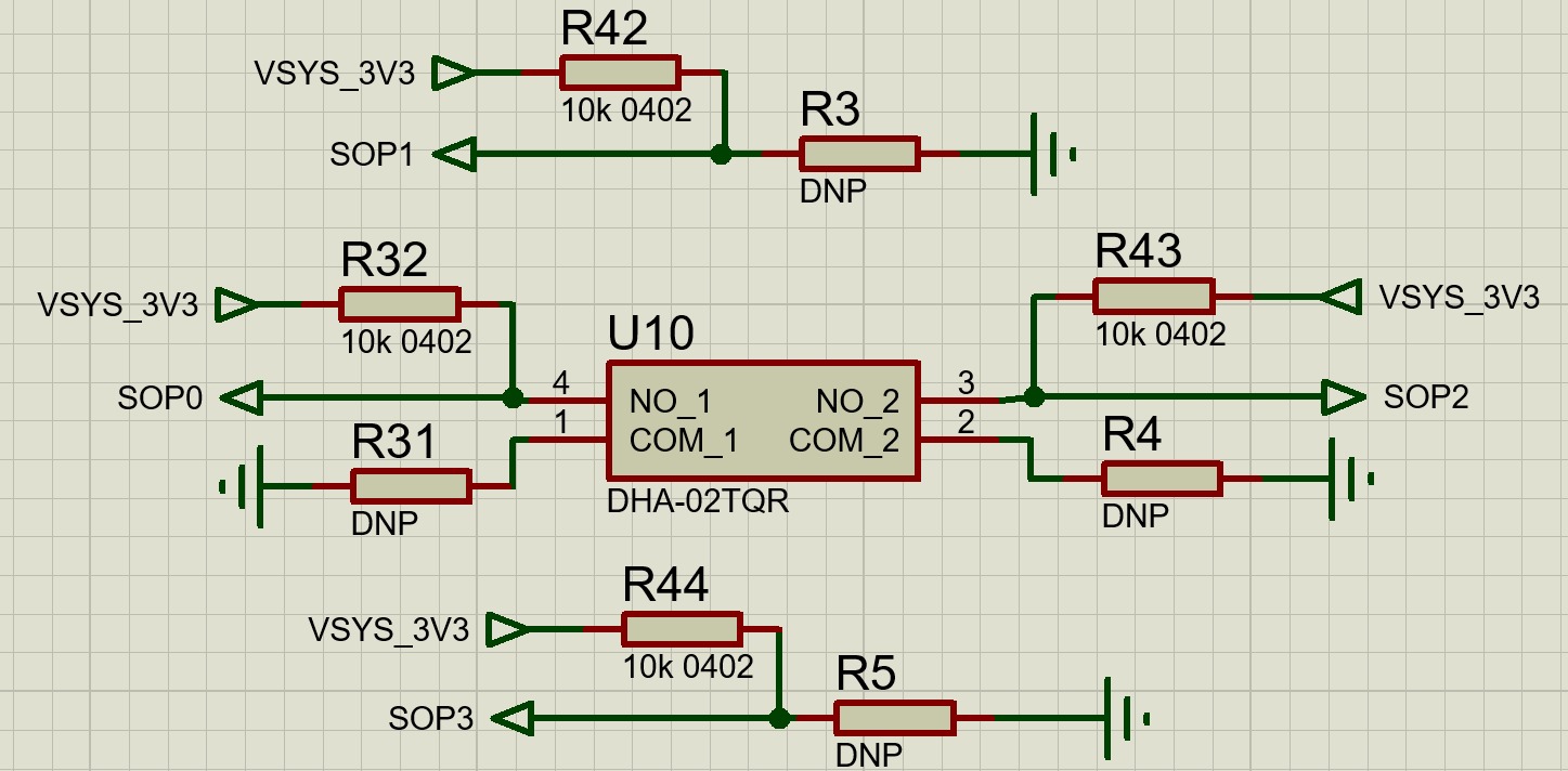
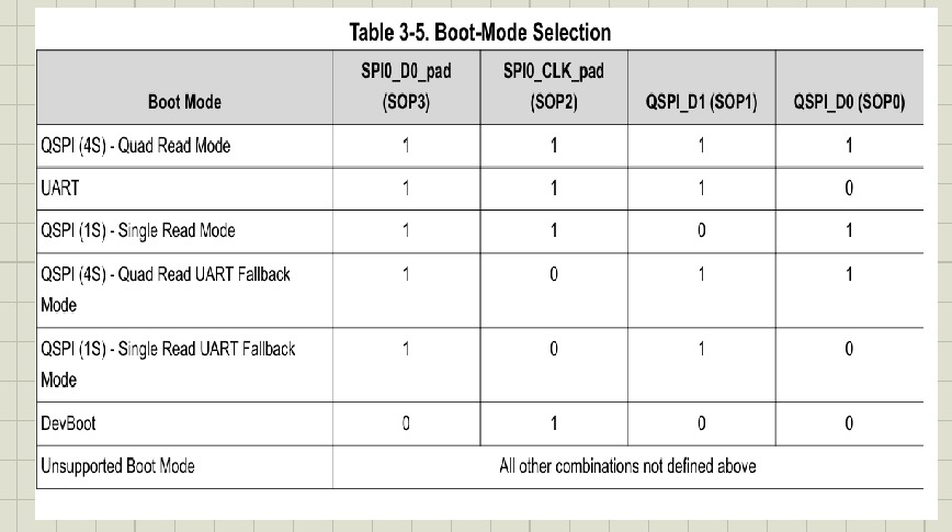
 Initially, the switches in the SOP selection circuit were configured for DevBoot according to the table shown below. I then tried the inverse configuration, because I was unsure whether the table indicated the switches’ open/closed states or the actual HIGH/LOW logic levels at the MCU’s SOP pins. Nonetheless, CCS reported the same DAP access error in both cases.

I have attached the SOP selection schematic and the boot-mode table below for reference. The pull-up and DNP resistor settings in the schematic were also changed and made compliant to DevBoot configuration.

I would also appreciate clarification on the table issue.AAA.jpegBBB.jpeg
  • Hi Baris,

    1. The table shows SOP pin logic levels, not switch positions

    Table 3-5 entries are the electrical levels sampled on SOP[3:0] at reset — 1 = 3.3V, 0 = GND 1. There is no universal "switch open = 1 / closed = 0" rule; TI states it is the designer's responsibility to translate the required logic levels into pull-up/pull-down and switch/jumper networks, and that boot-mode pins must never float 2. Which physical switch position produces a 0 depends entirely on which pull resistors you populate — so trace your own net, don't infer it from the table.

    The pins are latched once internal supplies stabilize and VDD_OK asserts (~2–6 ms window after PORz release, with tSU_SOP = 10 µs setup) 3. The switch only needs to hold a steady level through that window.

    2. Your schematic cannot produce a 0 on any SOP line as drawn

    From the attached schematic:

    Line Pull-up to VSYS_3V3 Path to GND Resulting level
    SOP0 R32 10k (populated) U10 NO_1 → COM_1 → R31 = DNP stuck 1
    SOP1 R42 10k (populated) R3 = DNP stuck 1
    SOP2 R43 10k (populated) U10 NO_2 → COM_2 → R4 = DNP stuck 1
    SOP3 R44 10k (populated) R5 = DNP stuck 1

    With R31/R4 unpopulated, toggling the DIP switch does nothing — the ground return is open. All four lines read 1111, which per your own Table 3-5 is QSPI (4S) Quad Read, not DevBoot. That explains why both switch orientations gave the identical result: electrically nothing changed. Fix: populate R31 and R4 (or install 0 Ω jumpers), then verify SOP[3:0] with a meter at the device pins while held in reset before attempting a connection.

    You mention the pull-up/DNP settings "were changed and made compliant" — the schematic provided still shows them DNP, so please confirm the physical board state.

    3. Yes — the unconnected 3.3V is a likely contributor

    JTAG with an LP-XDS110 is not functional on TCK/TMS/TDI/TDO/GND alone. The debugger needs a 3.3V IO reference to translate logic levels. In TI's LP-XDS110 reference setup, a jumper on the LP-XDS110 P9 connector (pins 2–3) is required so the target board supplies the 3.3V IO rail to the debugger 4. On other XDS110 hardware the same decision appears as the TGT VDD jumper — XDS when the debugger powers the target, EXT when the target powers itself; the wrong setting prevents correct JTAG operation 56. Since your board is self-powered, wire the target 3.3V to the debugger's IO-reference pin and leave the debugger from sourcing power.

    LP-XDS110 power jumper configuration 7

    4. Troubleshooting order

    1. Populate R31/R4, set the switch, probe SOP[3:0] at the pins during reset.
    2. Connect the 3.3V IO reference to the LP-XDS110 4.
    3. Verify all power rails (3.3V, 1.8V, 1.0V) and sequencing. A documented AM2634 case of Error -1170 + SC_ERR_PATH_BROKEN was root-caused to missing rails 8; another DAP-access case was traced to a core regulator sized at 50 mA against a >150 mA requirement 9. Confirm your rails hold under load, not just at idle.
    4. Handle TRST. The LP-XDS110 provides nRST, not TRST. In a resolved custom-board case the fix was to leave the debugger's nRST disconnected and pull the target's TRST high on the board 7. Check that your AM2634 TRSTn is not floating.
    5. Run Test Connection and confirm the JTAG DR Integrity scan test passes before trusting any DAP result — TI's custom AM263x bring-up FAQ specifies exactly this order: power rails → SOP levels → DR Integrity scan 10.
    6. Lower TCLK (e.g. 1 MHz) and power-cycle, per the standard guidance in the error text itself 9.
    7. Match XDS110 firmware to CCS. A -2131 (same DAP/register access family) case on CCS 20 was attributed to a firmware/emulation-package mismatch — CCS 20 requires firmware ≥ 3.0.0.36 where CCS 12.8 used 3.0.0.32 11. Worth checking on CCS 21.0.0.


    1. AM26x Hardware Design Guide (sprabj8d)
    2. AM263x Technical Reference Manual (spruj17i)
    3. AM26x Hardware Design Application Note (spradp6a) — SOP timing
    4. TI Reference Design LP-XDS110 debug setup (tidufc3)
    5. CC2662R-Q1 BCU-EVM User's Guide (swru641)
    6. LP-EM-CC35X1 User's Guide (swru629c)
    7. E2E: LP-XDS110 debug interface — TRST/nRST resolution
    8. E2E: AM2634 JTAG error connecting to brand new LP-AM2634
    9. E2E: LP-XDS110 debug/programming error -2131
    10. E2E FAQ: AM2634 board bring-up for custom AM263x/AM263Px PCB systems
    11. E2E: CCS12 → CCS20 debugger works intermittently
    12. AM26x Hardware Design Application Note (spradp6a) — boot modes

    Best Regards,

    Zackary Fleenor

  • Hello,

    I have previously used the LP-XDS110 debugger with the same debug connections I am using now, without connecting its 3V3 pin, and encountered no issues.

    The MCU receives power from another board connected to our Control Board, and all necessary MCU supply voltages are generated by regulators on the Control Board. We have verified that the 3.3 V rail is powered and at the expected voltage, and we have not observed any voltage drops that could affect the MCU. Would you still recommend connecting the debugger’s 3V3 pin to the board?

    Regarding SOP selection, the schematic below shows the actual circuit implemented on our board, which was configured according to the table shown below. As you explained, we understood the values in the table to represent the required logic levels at the SOP pins for each boot mode. The switches were configured accordingly, but we still encountered the same DAP access error.

    We also checked the reset pins shown in the other schematic and verified that they were all at logic HIGH, indicating that they were not being held in reset.

  • Hi Baris,

    Thanking you for the additional details addressing each question below:

    1. Is the 3V3 IO-reference pin still needed?

    Yes — recommend connecting it, even with your rail confirmed stable. The LP-XDS110's 3.3V pin isn't primarily a power source; it's the voltage reference the probe uses to translate TCK/TMS/TDI/TDO logic levels to match the target. In our reference designs, when the target is self-powered the debugger's jumper (labeled TGT VDD on the probe, or the P9 2–3 jumper on LP-XDS110) is set to EXT, meaning the target supplies this reference voltage to the probe rather than the probe sourcing power — this is a level-reference connection, not a power-draw risk to your regulators 1 2. Since your 3.3V rail is already verified stable, wiring it to the debugger only removes a variable; it should not introduce one. That said, if it previously worked without this connection on the same debug lines, the IO-reference pin is unlikely to be the root cause of the current -1170 — treat it as a cheap insurance step, not the primary suspect.

    2. Remaining causes for Error -1170 given corrected SOP and reset confirmed HIGH

    With SOP[3:0] now electrically correct for DevBoot and reset pins verified HIGH, the likely remaining culprits are:

    • Core/lock-step configuration: A documented AM2634 case produced this exact error (-1170, "Unable to access the DAP") only when connecting to Cortex_R5_1 or R5_3, while R5_0/R5_2 connected fine. Root cause was the default AM263x GEL script leaving the R5F subsystem in lock-step mode instead of dual-core — the second core of a locked pair is inaccessible to the debugger. Check the LOCK_STEP bit in MSS_CTRL_R5SSx_STATUS_REG via the Registers view, if you're targeting a specific core 3.
    • Power rails under load, not just idle: A separate AM2634 case with this same error plus SC_ERR_PATH_BROKEN was root-caused to missing/insufficient power rails (only one of four power LEDs lit) 4, and another DAP-access failure (same error family) traced to a core regulator undersized for current draw (50 mA supplied vs. >150 mA required) 5. Confirming voltage and current capability under JTAG-active load (not just idle multimeter reading) is important.
    • TRST floating: LP-XDS110 drives nRST, not TRST. If AM2634's TRSTn is left floating rather than pulled high on your board, the scan path can be unreliable even with correct SOP/reset.
    • XDS110 firmware vs. CCS 21.0.0 mismatch: A firmware/emulation-package mismatch in the same DAP-access error family was resolved by matching XDS110 firmware to the CCS version — CCS 20 required firmware ≥3.0.0.36 vs. the older 3.0.0.32 6.

    3. Next troubleshooting steps

    1. Check the LOCK_STEP bit if the failing core is R5_1 or R5_3.
    2. Verify TRSTn is pulled high on the board (not floating).
    3. Re-verify SOP[3:0] = 1011 at the device balls during reset — this is the confirmed DevBoot value 7.
    4. Confirm all rails (3.3V/1.8V/1.0V) hold under JTAG-active load, following TI's bring-up order: power rails → SOP levels → UART alive check → JTAG DevBoot → DR Integrity scan 8.
    5. Run Test Connection and confirm the JTAG DR Integrity scan-test succeeds before trusting any DAP result 9.
    6. Lower TCLK (e.g., 1 MHz) and power-cycle between attempts.
    7. Check/update XDS110 firmware for compatibility with CCS 21.0.0.
    8. Wire the target 3.3V to the LP-XDS110's IO-reference pin with the TGT VDD/P9 jumper set for target-powered (EXT) operation.

    Can you confirm which R5F core you're attempting to connect to first (R5_0 or another), and whether you can share the Test Connection / JTAG DR Integrity scan-test log?

    1. LP-XDS110 User's Guide
    2. LP-EM-CC35X1 User's Guide
    3. E2E: AM2634 Error -1170 lock-step core access
    4. E2E: AM2634 JTAG error on brand new LP-AM2634
    5. E2E: LP-XDS110 Error -2131 regulator sizing
    6. E2E: CCS12→CCS20 firmware mismatch
    7. AM26x Hardware Design Application Note — Boot Modes
    8. E2E FAQ: AM2634 Board Bring-up for Custom AM263x/AM263Px PCBs
    9. AM26x Hardware Design Application Note — JTAG Verification

    Best Regards,

    Zackary Fleenor