- Ask a related questionWhat is a related question?A related question is a question created from another question. When the related question is created, it will be automatically linked to the original question.
This thread has been locked.
If you have a related question, please click the "Ask a related question" button in the top right corner. The newly created question will be automatically linked to this question.
Hi,
I am working on board layout based on DM8148 and was referring to layout guideline given in the datasheet for DDR3 placement and routing. Related to those guidelines I have one query related to DDR3 chip placement on board.
My question :
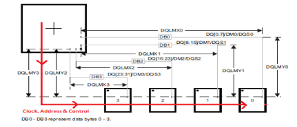
Which DDR3 chip should be placed near to processor? Lower data byte or higher data byte? Or it is irrespective which DDR3 chip is placed near to processor. Below snapshot from datasheet will clarify my question further.

Above snapshot is taken from DM8148 datasheet page 317 under section "8.13.4.2.4.15.2 DQS and DQ Routing Specification". This section is related to routing guideline of data and DQS signals. Above snapshot shows lower data byte DDR chip is placed far from the processor and highest data byte DDR chip is placed nearest to processor. I have shown the routing of clock, control and address bus with red line which denotes clock will be routed first to higher data byte DDR and last in lower data byte DDR. Is this placement and routing of DDR3 correct? Or it is irrespective which data byte DDR placed near to processor and which DDR placed far from processor?
Thanks,
M
M,
As you can see in the diagram you post above the low byte is furthest away. This is not critical, but the escape routing from the processor should mean that this is the easiest configuration.
What is critical is that the DQS/M/data signals are matched correctly as per the datasheet.
BR,
Steve
Thanks Steve,
Referring to your reply I am concluding that higher data byte DDR can be placed nearer to processor and lower data byte DDR can be placed far from processor. Only important factor is to length match DQS/M/data lines respectively.
So I believe, the routing strategy for clock, control and address bus shown in snapshot will do the work. Here, clock will be routed to higher data byte DDR first and will be terminated after last DDR which is the lower data byte DDR. Please confirm.
BR,
M
Yes, as shown in the diagram this is how it is intended for the flyby topology.
BR,
Steve