- Ask a related questionWhat is a related question?A related question is a question created from another question. When the related question is created, it will be automatically linked to the original question.


hello TI-friends,
after checking http://processors.wiki.ti.com/index.php/DM816x_C6A816x_AM389x_DDR3_Init
we got value as below
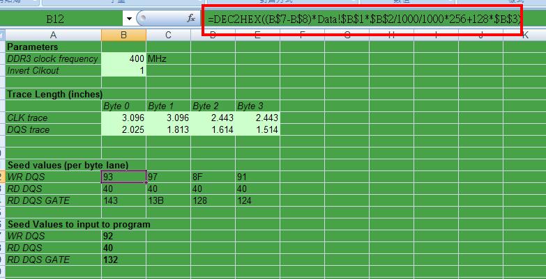
| DDR3 clock frequency | 400 | MHz | ||
| Invert Clkout | 0 | |||
| Trace Length (inches) | ||||
| Byte 0 | Byte 1 | Byte 2 | Byte 3 | |
| CLK trace | 3.096 | 3.096 | 2.443 | 2.443 |
| DQS trace | 2.025 | 1.813 | 1.614 | 1.514 |
| Seed values (per byte lane) | ||||
| WR DQS | 13 | 17 | F | 11 |
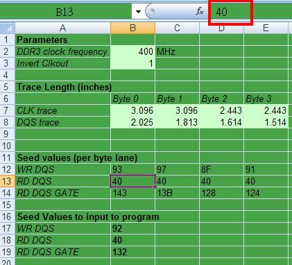
| RD DQS | 40 | 40 | 40 | 40 |
| RD DQS GATE | C3 | BB | A8 | A4 |
| Seed Values to input to program | ||||
| WR DQS | 12 | |||
| RD DQS | 40 | |||
| RD DQS GATE | B2 | |||
in arch/arm/include/asm/arch-ti81xx/ddr_defs_ti816x.h.
#define RD_DQS_GATE_LANE3 does this map to C3 or A4 ??