This thread has been locked.

If you have a related question, please click the "Ask a related question" button in the top right corner. The newly created question will be automatically linked to this question.

Need help in GPIO usage as output pin.

Other Parts Discussed in Thread: TMS320C6748

Hello,

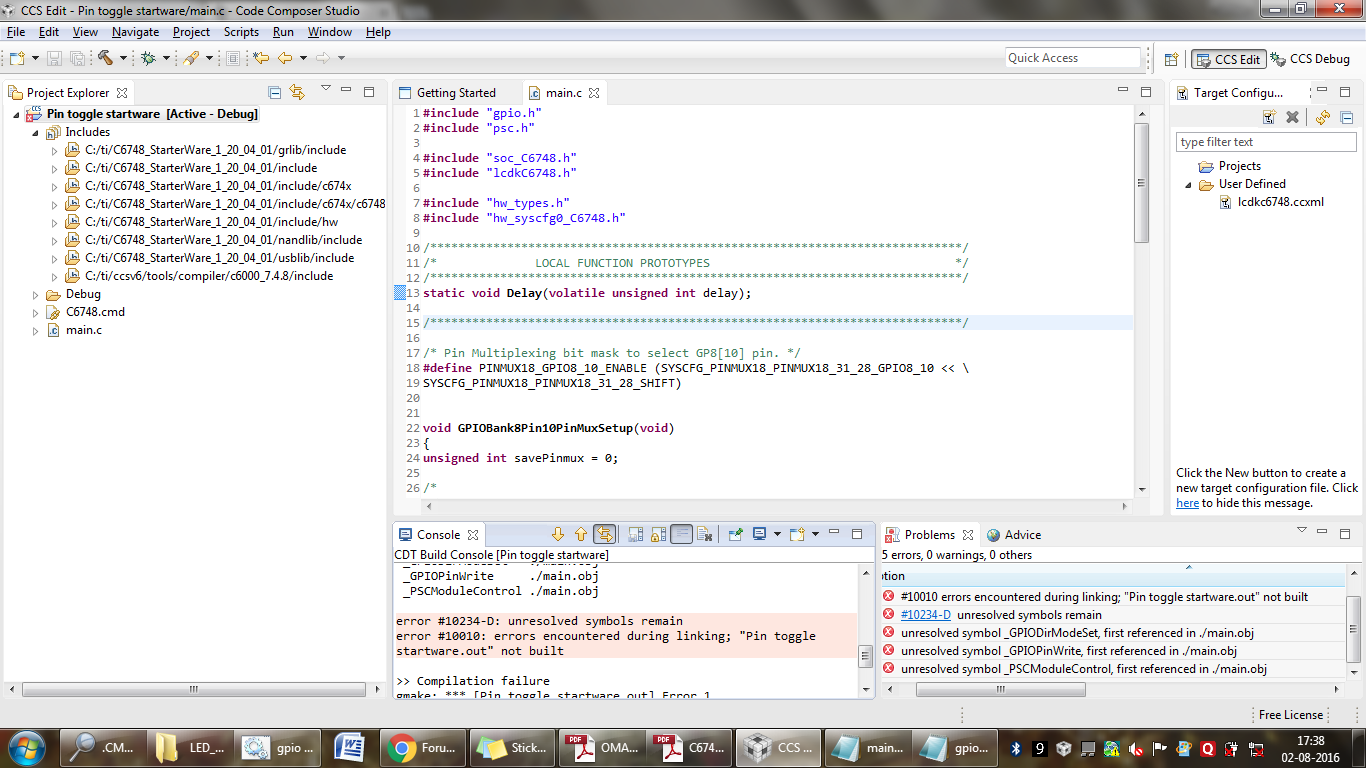
I am writing a program for generating a square wave using TMS320LCDKC6748 DSP processor's GPIO.

Could you please help in memory mapping of GPIO and all support files and directories needed to be added.

Pin toggle.docx.

Please also let me know if any setting regarding memory allocation needs to be done.

Additional info: Windows 7 64-bit, Service Pack 1, Code Composer Studio Version: 6.0.1.00040

Thanks,

Onkar

  • Onkar,

    Typically the memory map for TI device is found in the Technical reference manual and the data manual for the processor which you can find here:
    www.ti.com/.../TMS320C6748

    If you are looking for software where this has already been defined then I would recommend, you look at the Starterware package :
    processors.wiki.ti.com/.../StarterWare

    what you are trying to implement should be easy to implement. Find the GPIO pin on the board that you will connect to the scope in the board schematics for LCDK:
    www.ti.com/.../TMDSLCDK6748 Documents

    In you code, power up the GPIO module using PSC module, configure the pinmux register, configure the required pin as output and the write to the GPIO register when you want the signal to go high, use a counter or a device timer to configure the time based on the duty cycle you need and then toggle the GPIO to zero.

    If you search the forums, you should be able to find a good starting point for implementing this functionality from other community developers who may have implemented something similar.

    Regards,
    Rahul
  • Hi ONKAR,

    Here is the sample code for configuring the GPIOs.

  • OMAP-L138 LC DEV KIT VER A7E.pdfGPIO example issue.docxtms320c6748_datasheet.pdfC6748_user_manual.pdfHello Shankari,

    Thanks for reply.

    I tried example from Startware, here is the path -> C:\ti\C6748_StarterWare_1_20_04_01\build\c674x\cgt_ccs\c6748\lcdkC6748\gpio.

    When I imported this project directly in the CCS it compiled correctly.

    But when I created new ccs project and copied same code with same directories included it gave errors.

    please find attached screenshots.

    Actually I want to interface an ADC to any of the GPIO pin.

    Hence I am trying to access any GPIO pin on the TMS320C6748 LCDK board and trying to toggle it and get the square wave on the oscilloscope as  a test.

    But I am not able to link pins in the schematic of the board (which are represented as J14 (46 pins)and J15 (46 pins) on the board )and corresponding pinmux and actual pin number in the datasheet. Please find attached the same as well.

    Could you please help me to identify the same.

    Also the function for Pin Multiplexing of pin 12 of GPIO Bank 6 is given as  GPIOBank6Pin12PinMuxSetup(); in the example.

    Similarly what are the functions for pin no.22 in the J15 module of the schematic which is referred as GPIO8-10.  

    Is it ok if I use it  to toggle it and get the square wave on the oscilloscope as  a test and then use it for interfacing the ADC.

    Thanks,

    Onkar

  • Onkar,

    onkar said:
    Also the function for Pin Multiplexing of pin 12 of GPIO Bank 6 is given as GPIOBank6Pin12PinMuxSetup(); in the example.
    Similarly what are the functions for pin no.22 in the J15 module of the schematic which is referred as GPIO8-10.


    Yes, you can write a similar Pinmux function for GPIO8[10] like below:


    /* Pin Multiplexing bit mask to select GP6[12] pin. */
    #define PINMUX18_GPIO8_10_ENABLE (SYSCFG_PINMUX18_PINMUX18_31_28_GPIO8_10 << \
    SYSCFG_PINMUX18_PINMUX18_31_28_SHIFT)


    void GPIOBank8Pin10PinMuxSetup(void)
    {
    unsigned int savePinmux = 0;

    /*
    ** Clearing the bit in context and retaining the other bit values
    ** in PINMUX13 register.
    */
    savePinmux = (HWREG(SOC_SYSCFG_0_REGS + SYSCFG0_PINMUX(18)) &
    ~(SYSCFG_PINMUX18_PINMUX18_31_28));

    /* Setting the pins corresponding to GP6[12] in PINMUX13 register.*/
    HWREG(SOC_SYSCFG_0_REGS + SYSCFG0_PINMUX(18)) =
    (PINMUX18_GPIO8_10_ENABLE | savePinmux);

    }

    But I am not able to link pins in the schematic of the board (which are represented as J14 (46 pins)and J15 (46 pins) on the board )and corresponding pinmux and actual pin number in the datasheet. Please find attached the same as well.


    In the schematics, search as GPIO8[10] and in TRM search as GP8[10], which will give you the PINMUX register number as well as the value to select the GPIO.
  • Hello Shankari,

    Thanks for above clarification.

    But getting some issues regarding linking.

    I tried to link with C6748.cmd and also with gpio.cmd from StarterWare as below.

    C:\ti\C6748_StarterWare_1_20_04_01\build\c674x\cgt_ccs\c6748\lcdkC6748\gpio

    But for both I am getting errors.

    Could you please help me with this.

    Thanks,

    Onkar

    Code:-

    #include "gpio.h"
    #include "psc.h"

    #include "soc_C6748.h"
    #include "lcdkC6748.h"

    #include "hw_types.h"
    #include "hw_syscfg0_C6748.h"

    /****************************************************************************/
    /* LOCAL FUNCTION PROTOTYPES */
    /****************************************************************************/
    static void Delay(volatile unsigned int delay);

    /****************************************************************************/

    /* Pin Multiplexing bit mask to select GP8[10] pin. */
    #define PINMUX18_GPIO8_10_ENABLE (SYSCFG_PINMUX18_PINMUX18_31_28_GPIO8_10 << \
    SYSCFG_PINMUX18_PINMUX18_31_28_SHIFT)


    void GPIOBank8Pin10PinMuxSetup(void)
    {
    unsigned int savePinmux = 0;

    /*
    ** Clearing the bit in context and retaining the other bit values
    ** in PINMUX13 register.
    */
    savePinmux = (HWREG(SOC_SYSCFG_0_REGS + SYSCFG0_PINMUX(18)) & ~(SYSCFG_PINMUX18_PINMUX18_31_28));

    /* Setting the pins corresponding to GP6[12] in PINMUX13 register.*/
    HWREG(SOC_SYSCFG_0_REGS + SYSCFG0_PINMUX(18)) = (PINMUX18_GPIO8_10_ENABLE | savePinmux);

    }

    /*****************************************************************************/
    int main(void)
    {


    /* The Local PSC number for GPIO is 3. GPIO belongs to PSC1 module.*/
    PSCModuleControl(SOC_PSC_1_REGS, HW_PSC_GPIO, PSC_POWERDOMAIN_ALWAYS_ON,
    PSC_MDCTL_NEXT_ENABLE);

    /* Pin Multiplexing of pin 12 of GPIO Bank 6.*/
    GPIOBank8Pin10PinMuxSetup();

    /* Sets the pin 109 (GP6[12]) as input.*/
    GPIODirModeSet(SOC_GPIO_0_REGS, 139, GPIO_DIR_OUTPUT);

    while(1)
    {
    GPIOPinWrite(SOC_GPIO_0_REGS, 139, GPIO_PIN_LOW);

    Delay(1000000);

    GPIOPinWrite(SOC_GPIO_0_REGS, 139, GPIO_PIN_HIGH);

    Delay(1000000);
    }


    }

    /*
    ** \brief This function can be called to generate a delay.
    */

    static void Delay(volatile unsigned int delay)
    {
    while(delay--);
    }


    /*****************************END OF FILE************************************/

  • Hello, 

    In continuation with above query,

    I think I am not able to link proper .lib files in File search path.

    Could you please tell me names and location of those files in StarterWare because there are many .lib files in the starterWare.

    And I am not sure which are to be included.

    Thanks,

    Onkar

  • i am also facing the same trouble in mapping GPIO as well i want use uPP available with LCDK c6748 board so that i can communicate the other electronic with help of 16 bit parallel ADC with DSP, i have tried to install uPP driver in my system but it is not getting install successfully .

    in mean while i tried to do some experiment with Starter ware software also i couldn't able to locate library files
    also .
    please guide me too regarding GPIO, and parallel ADC compatibility with c6748.

    thank you.

    additional info.: windows 10 system , CCS 6.0 .1 version