This thread has been locked.

If you have a related question, please click the "Ask a related question" button in the top right corner. The newly created question will be automatically linked to this question.

DRA64x_HDVPSS: Delay of HSYNC and VSYNC adjustment for vout

Other Parts Discussed in Thread: CCSTUDIO

Dear expert 

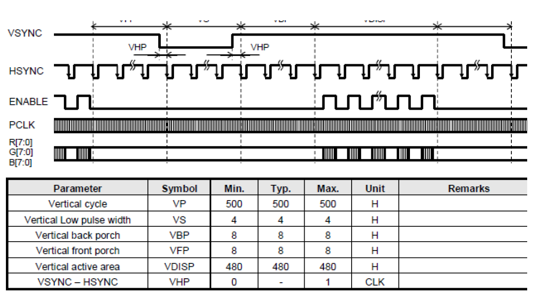
Our customer observed delay of HSYNC and VSYNC of vout is about 385 pclk in DRA64x. however the delay of HSYNC and VSYNC is expected to <1 pclk. Here is snapshot of HSYC and VSYNC.  Did you have any idea to adjust the delay time?  I have asked them to try invert polarity of VSYNC/HSYNC. It does NOT work.

Regards

Dong

  • Hi Dong,

    Dong Yang said:
    Our customer observed delay of HSYNC and VSYNC of vout is about 385 pclk in DRA64x. however the delay of HSYNC and VSYNC is expected to <1 pclk.

    The max and min delay time of VOUT[x]_CLK to VOUT[x]_HSYNC and VOUT[x]_VSYNC is provided in DRA64x datasheet (SPRS694B),

    Table 8-44. Switching Characteristics Over Recommended Operating Conditions for HDVPSS Output

    td(CLK-VSYNC) - Delay time, VOUT[x]_CLK low (falling) to control valid:  -1.2ns to 2ns

    td(CLK-HSYNC) - Delay time, VOUT[x]_CLK low (falling) to control valid:  -1.2ns to 2ns

    Figure 8-40. HDVPSS Output Timing

    Dong Yang said:
     Did you have any idea to adjust the delay time?  I have asked them to try invert polarity of VSYNC/HSYNC. It does NOT work.

    Please see the below errata and e2e threads:

    Advisory 3.0.24   HDVPSS VOUT[x]_CLK: Does Not Support Positive-Edge Clocking


    Regards,
    Pavel

  • Pavel,
    Thanks for your reply.
    1) I'm talking about the delay between HSYNC and VSYNC instead delay between HSYNC and CLK.
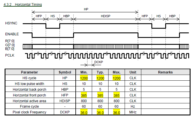
    The VESA timing, The faling edge of HSYNC and VSYNC are aligned. However the above snapshot shows HSYNC and VSYNC delay is 381 nclk as I configure Horizontal back porch = 5 and Horizontal front porch = 385;
    The delay between HSYNC and VSYNC delay is less than 1 nclk as I configure Horizontal back porch = 390 and Horizontal front porch = 0; However it is against TFT LCD's spec which is required Horizontal back porch = 5 and Horizontal front porch = 385.
    2) Can you help to explain DVO and OSD timing setting in HD_VENC? How they impact the output timing?

    Regards
    Dong
  • Hi Dong,

    DRA64x (DM814x) TI EVM comes with 7 inch TFT RGB LCD with resolution of 800x480, and the EZSDK/PSP support this LCD. Can you provide more details regarding your custom LCD?

    The easiest way to adjust the display timings for custom LCD is through sysfs entries, see the below wiki page for more info:

    processors.wiki.ti.com/.../TI81XX_PSP_VPSS_Video_Driver_User_Guide

    See also the below wiki pages and e2e threads which discuss display timing adjustment (hsync, vsync, etc) for custom LCD:

    processors.wiki.ti.com/.../Sitara_Linux_LCDC_Porting_Guide
    processors.wiki.ti.com/.../Adding_new_DVI_resolutions
    processors.wiki.ti.com/.../OMAP3_DSS2_Architecture
    processors.wiki.ti.com/.../LCD_RGB_640x480_VGA_Addition

    e2e.ti.com/.../915028
    e2e.ti.com/.../915026
    e2e.ti.com/.../336084
    e2e.ti.com/.../282107
    e2e.ti.com/.../312716

    Regards,
    Pavel
  • Pavel,

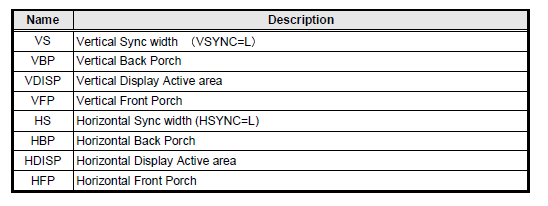
    I go though the link you haved shared. The logic for display timing is similar though customer is using QNX.  It is controlled by below 8 parameters in HDVPSS. I was able to get display out. How can I corelate the 8 pamaters to delay of HSYNC and VSYNC?  From my understanding,  The faling edge of VSYNC and HSYC are aligned by default.  However the output from HDVPSS is NOT  aligned.

    Regards

    Dong

  • Dong,

    You should refer to the HDVPSS User's Guide SPRUHF7B, see sections:
    1.2.7 High-Definition Video Encoder (HD_VENC)
    1.3.9 HD_VENC_D Registers

    You might also get as a reference the CCStudio based code for the DM814x TI EVM LCD settings.

    www.mistralsolutions.com/.../tmdxevm8148.html

    SOFTWARE -> Diagnostic Software -> Expansion I/O Board -> Rev D -> src -> CCS_Test_Code -> IOExpansion_Application -> lcd_display

    The HDVPSS HD_VENC registers are defined in vpss.h and configured in vpss.c files.

    HDVPSS base address is 0x48100000. HD_VENC_D_DVO2 offset is 0xA000.

    Regards,
    Pavel
  • Pavel,

    Thanks for your response.

    I can not find any register to adjust aligment of HSYNC and VSYNC.  Could you help to explain the relationship between aligment of HSYNC/VSYNC and the 8 pamameter(front porch, sync width, back portch etc) in abovesnapshot?

    Regards

    Dong

  • You might also run TI PSP linux kernel on your board, set the desired mode, output and timings on your custom board using the VPSS driver though sysfs entries, and when you get the correct LCD settings, you can dump the HDVPSS registers and apply the values there in your QNX code base.

    For more info you can refer to the HDVPSS wiki page:
    processors.wiki.ti.com/.../TI81XX_PSP_VPSS_Video_Driver_User_Guide

    The supported modes are located in linux-kernel/drivers/video/ti81xx/vpss/sysfs.h

    #echo <mode> > /sys/devices/platform/vpss/display1/mode

    #echo <display timings> > /sys/devices/platform/vpss/display1/timings

    #echo <output> > /sys/devices/platform/vpss/display1/output

    Regards,
    Pavel
  • Hi Dong,

    What is this platform DRA64x?
    I dont see any registers in the venc to aligh hsync and vsync, so it is very difficult. There might be something present in the control module. But first tell me know which is this platform?

    Regards,
    Brijesh
  • Hi Dong,

    VSYNC switch always when the internal pixel counter=0 for non-interlaced mode.
    HSYNC switch at pixel counter = DVO_HS_ST.

    Please check DVO_HS_ST and DVO_HS_WD parameters in the HD_VENC configuration registers to see if settings of these two parameter cause the HSYNC switch delay.

    If the settings are not correct, probably need to understand why the setting is not correct in the first place (since there might be a reason for the skew in the first place).

    Regards,
    Brian
  • Brijesh,
    DRA64x is DM8148 platform.

    Regards
    dong
  • Brain

    Thanks for your response. Your response is exactly what I'm looking for.

    Can you advise how to check DVO_HS_ST and DVO_HS_WD parameters ?

    What's the difference between OSD and DVO interface? Shoud I configure DVO_HS_ST or OSD_HS_ST etc to meet below required timing from LCD?

    Regards

    Dong

  • Dong,

    >> Can you advise how to check DVO_HS_ST and DVO_HS_WD parameters ?

    These are defined in HD_VENC_D_CFG15 and CFG16 registers. (Can you point me to the TRM that you are using so that I can point out specific section?)

    As for OSD and DVO, OSD is for generating sync for internal module and DVO is for external interface. Generally, these can be the same.

    Can you please have the customer dump the HD_VENC module cfg registers?

    Regards,
    Brian
  • Brain

    Here is register dump of hvpss_hd_venc_d: base=4810a000

    offset=0x0       0x41832033

    offset=0x4       0x0

    offset=0x8       0x0

    offset=0xc       0x0

    offset=0x10      0x0

    offset=0x14      0x0

    offset=0x18      0x0

    offset=0x1c      0x0

    offset=0x20      0x0

    offset=0x24      0x0

    offset=0x28      0x841f44b0

    offset=0x2c      0x1f000013

    offset=0x30      0xa32018f

    offset=0x34      0x0

    offset=0x38      0x0

    offset=0x3c      0xa320190

    offset=0x40      0x14181

    offset=0x44      0x1e0000

    offset=0x48      0x4008000

    offset=0x4c      0x0

    offset=0x50      0x0

    offset=0x54      0xa320188

    offset=0x58      0x14181

    offset=0x5c      0x1e0000

    offset=0x60      0x4008000

    offset=0x64      0x0

    offset=0x68      0x0

    Regards

    Dong

  • Hi Dong,
    Is this issue resolved now by changing cfg15/16 registers?

    Rgds,
    Brijesh
  • Brijesh
    The issue is not rosolved by changing cfg15/16 registers. I have dump the register cfg15/cfg16(offset=0x3c and offset=0x40) as above. Can you help to add your comments?

    Regards
    Dong
  • Brian
    The new cfg is working on customer’s board. They can get complete display and HSYNC/VSNYC aligned from scope.

    The new cfg is:

    WR 4 0
    WR 8 0
    WR c 0
    WR 10 0
    WR 14 0
    WR 18 0
    WR 1c 0
    WR 20 0
    WR 24 0
    WR 28 841f44b0
    WR 2c 1f000013
    WR 30 a320000
    WR 34 0
    WR 38 0
    WR 3c a32000f  cfg[15]
    WR 40 14000  cfg[16]
    WR 44 1e0000
    WR 48 4008000
    WR 4c 8000
    WR 50 0
    WR 54 a320007  cfg[21]
    WR 58 14000
    WR 5c 1e0000
    WR 60 4008000
    WR 64 0
    WR 68 0
    WR 0 41832033

    Regards
    Dong
  • Dong,

    Just to recap the changes required to align Vsync/Hsync:

    There is an internal counter used by the Video Encoder to switch VSYNC and HSYNC sync outputs.

    The VSYNC always switches when the counter = 0.

    Therefore, HSYNC switching time needs to be set up so that HSYNC also switches at the counter = 0.

    This is set up by setting  cfg16_DVO_HS_ST=0.

    With this parameter changed,  following two parameters must be changed to match the new setting:

    cfg15_DVO_AVST_H =   HS + HBP   (Hsync pulse width and Horizontal Back Porch period)   --> to set when the video output should be generated with respect to the HSYNC.

    cfg21_OSD_AVST_H = DVO_AVST_H - 8  (to set internal module timing with respect to the adjusted DVO_AVST_H.

    This information should be applicable for any progressive RGB output display output configuration.

    Regards,

    Brian