This thread has been locked.

If you have a related question, please click the "Ask a related question" button in the top right corner. The newly created question will be automatically linked to this question.

AM5708: EVM design questions

Part Number: AM5708
Other Parts Discussed in Thread: LP873220, TPS22965, TPS22954

All, 

I do have several questions on the AM5708 EVM schematic "518202_DRA71x_DRA79x_TDA2Ex17_AM570x_EVM_OrCAD_PDF_Rev_C_24OCT2016.pdf".

- On the DDR power supply side, why the schematic has been populated with U72 (page 8)?

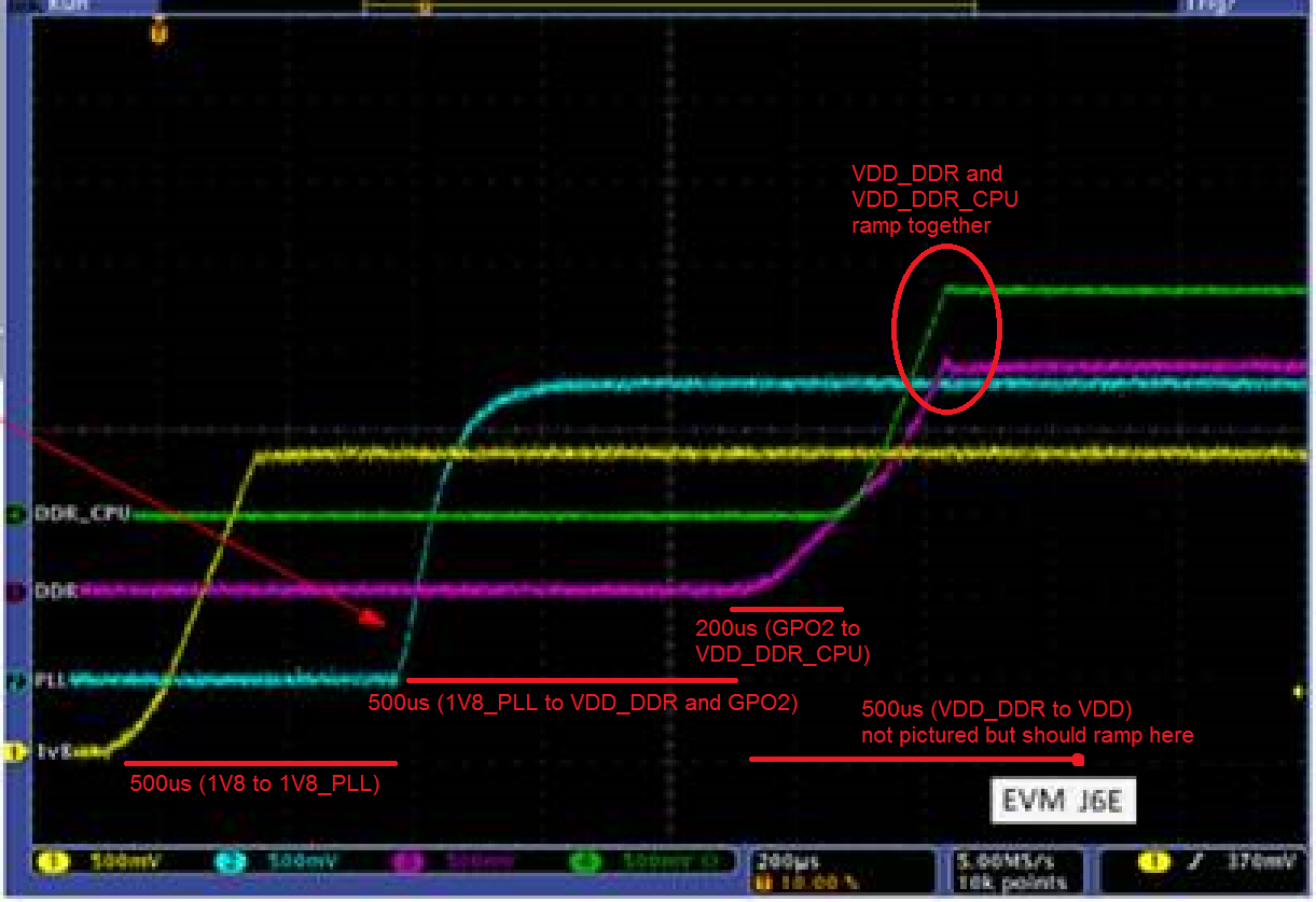
  • DDR3 modules are powered-up by BUCK1 of the LP8732x (VDD_DDR) through a power monitor sensing resistor
  • The AM5708 VDDS_DDR1 is powered-up by VDD_DDR_CPU (through a power monitor sensing resistor) generated by U72 from VDD_DDR

You're familiar with the power-up and power-down sequencing (page 7 - SNVU554-May17) of the LP8733x (version 0x2D) and the LP8732x (version 0x20) – our EVM makes use of the 0x2A and 0x2E verisons. 

Looking at our schematic there’s a 0.8ms delay between VDD_DDR_CPU and VDD_DDR due to U72 meaning VDDS_DDR1 comes up 1.8ms later than the PMIC and so 0.3ms later than VDD (+1.15V): 

-  0.0ms: PMICs enable (EN signal in the attached pdf)

-  1.0ms: VDD_DDR is generated (LP873220_BUCK1) to power up the DDR3 modules and at the same time U72 is enabled through LP873220_GPO2

-  1.5ms: VDD (LP97332D_BUCK0) is generated

-  1.8ms: VDD_DDR_CPU is generated by U72 to power-up the AM5708 VDDS_DDR1

This looks like in contrast with the AM570x datasheet (pag. 153 - SPRS961A-Feb17) where VDDS_DDR1 should come up before VDD – what do you think?

Last but not least, looking at the schematic there’s one more switch (U122 at page 14) to control the microSD power supply.

According to the microSD specs, in order to modify the operating voltage of the card it’s necessary an ON/OFF cycle. Same story holds true to get access to cards that have reached an inactivity during the initialization phase in “SD mode”. 

Since according the application requirements, the microSD card is always powered-up at 3.3V and initialized in “SPI mode”, there shouldn’t be any need for cycling the power. If so, I could avoid using the switch and tie the microSD power supply to VDDSHV8 generated by LDO0 of the LP8733x – how do you feel about that?

Please let me know - it's an urgent matter.

Thanks in advance for your kind support.

  • The factory team have been notified. They will respond here.
  • Hello Fabio,

    The TPS22965 load switch (U72 on pg 8) is optional. Its purpose is to separate the SoC DDR rail from the DDR memory modules. The SoC can be powered down while the DDR memory modules remain powered and set to "self-refresh". The load switch is optional and can be excluded in the final design if your end product will not support "suspend to RAM".

    An alternative (faster) load switch with a delay of only 300 us will be the TPS22954 with Ct = 0. That should allow enough time for the VDD rail to sequence after.

    Regarding the microSD card you can definitely avoid the extra LDO and keep the SD card in 3.3V mode only. To make sure the SoC does not try to negotiate the 1.8V mode you will need to remove the UHS high speed modes from the Linux Device Tree (dts) file. 

    Regards,
    Ahmad

  • Ahmad,

    many thanks for your prompt reply - appreciated!

    There a missing answer yet - please find it below:

    You're familiar with the power-up and power-down sequencing (page 7 - SNVU554-May17) of the LP8733x (version 0x2D) and the LP8732x (version 0x20) – our EVM makes use of the 0x2A and 0x2E verisons. 

    Looking at our schematic there’s a 0.8ms delay between VDD_DDR_CPU and VDD_DDR due to U72 meaning VDDS_DDR1 comes up 1.8ms later than the PMIC and so 0.3ms later than VDD (+1.15V): 

    -  0.0ms: PMICs enable (EN signal in the attached pdf)

    -  1.0ms: VDD_DDR is generated (LP873220_BUCK1) to power up the DDR3 modules and at the same time U72 is enabled through LP873220_GPO2

    -  1.5ms: VDD (LP97332D_BUCK0) is generated

    -  1.8ms: VDD_DDR_CPU is generated by U72 to power-up the AM5708 VDDS_DDR1

    This looks like in contrast with the AM570x datasheet (pag. 153 - SPRS961A-Feb17) where VDDS_DDR1 should come up before VDD – what do you think?

    Can you please comment?

    Thanks

  • Hi Fabio,
    Actually we do not support "suspend to RAM" at all. Meaning U72 must be removed. If you remove U72 and connect the VDD_DDR_CPU and VDD_DDR together. That will solve the power sequencing problem. In the rare occurrence that you need this feature then you should take the part recommendation from my previous post (TPS22954).

  • Hi Fabio,

    I have an update regarding the timing of U72 / TPS22965. I was able to obtain the osciliscope captures that validated the power sequencing and it appears that the delay between VDD_DDR and VDD_DDR_CPU is only 200us. Therefore VDD still has time to ramp after VDD_DDR and VDD_DDR_CPU. I hope this alleviates your concern.