This thread has been locked.

If you have a related question, please click the "Ask a related question" button in the top right corner. The newly created question will be automatically linked to this question.

CCS/66AK2G12: The reason memory and memory map of DDR3 do not match.

Other Parts Discussed in Thread: 66AK2G12

rt Number: 66AK2G12

Tool/software: Code Composer Studio

Dear Sir,

Currently, We develop our product using 66AK2G12, And debug the DDR3.

So we are trying to our firmware load to DDR3 directly via JTAG and CCS.

But there is some problem happen.
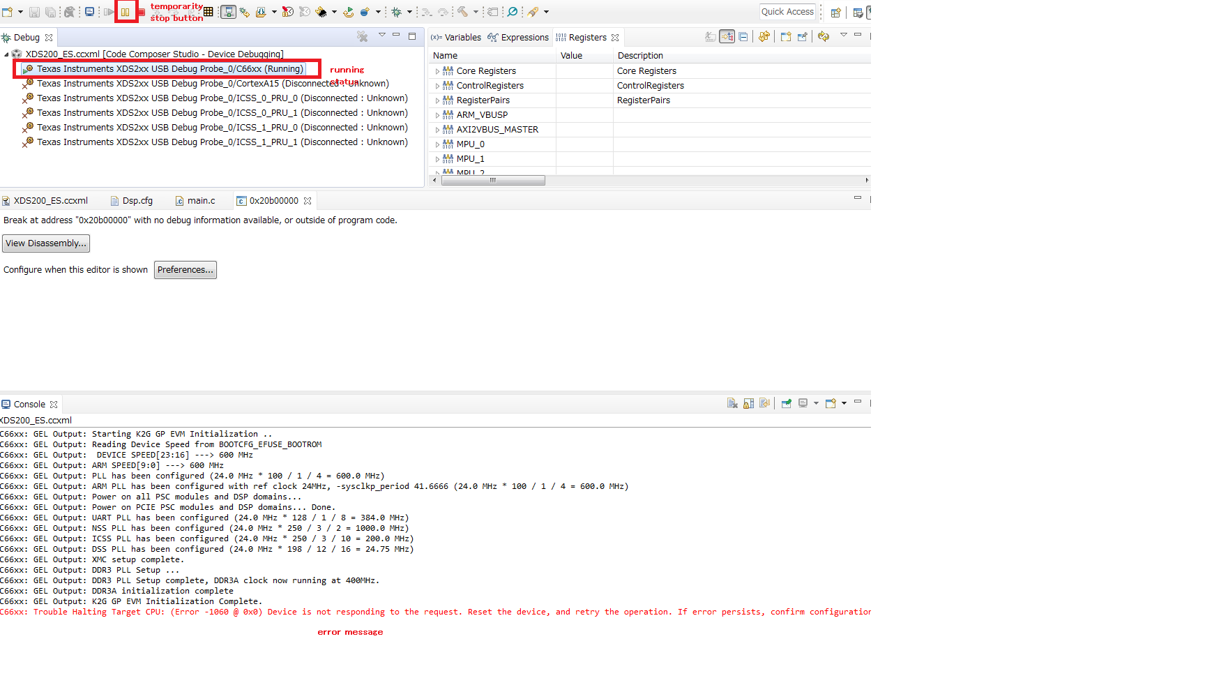
The error comment display on CCS. Please check attached file
(Below is error comment).

C66xx: File Loader: Verification failed: Values at address 0x81320568 do not match Please verify target memory and memory map.
C66xx: GEL: File: D:\test.out: a data verification error occurred, file load failed.

If we change the object attrs from "r--" to "rw-" ,This problem did not happen.

So we confirmed whether this phenomenon occurs when the attributes of the object are changed.(from "r--" to "rw-" / from "r--" to "rw-")
In the end,we noticed that this phenomenon occurs the "r--" object.

Please tell us the reason why is this phenomenon happen and what should we investigate. we have already finished the DDR3 read and write hardware check.

  • I am not sure at the moment if the issue is SW or HW related and will need a little more information about your board DDR verification process.

    1. Can you confirm that you have used the EMIF tools that we provide here for the EMIF SDRAMTiming and HW levelling? 

    http://software-dl.ti.com/processor-sdk-rtos/esd/docs/latest/rtos/FAQ.html#useful-ddr-configuration-resources

    2. How was the DDR read writes verified. Did you use memtest from uboot or diagnostic test. Did you check that over the entire DDR range ?

    3. Do you see the same behavior from ARM and DSP when accessing that region. Can you open memory browser and from the memory window read and write to that location. 

    4. Please confirm if DDR ECC is enabled? Are you setting DDR to 1066 or 800 MTs speeds. Check GEL file to confirm there is no memory map setting for that region for the emulator (Refer section 4 here http://www.ti.com/lit/an/spraa74a/spraa74a.pdf)

    Regards,

    Rahul

  • Dear Rahul,

    Thank you for your advise.

    First, We report our situation.

    For DDR3 settings, Our product  is using the K2 DDR3 Register Calc v1p60.xlsx (Sprabx7). using only one chip.

    And the  DDR3 is  MT41K256M16-125-96FBGA. The DDR3 can selected in the K2 DDR3 Register Calc v1p60.xlsx. 

    We changed the item of K2 DDR3 Register Calc v1p60.xlsx  is below.

    ■The DDR3  Output Clock Freqency  is 400MHz.

    ■The Device is MT41K256M16 125(1600).

    ■The CAS_WRITE_LATENCY is CWL = 6.

    ■The Narrow Mode is 16-bit bus width

    ■THe ECC Byte is DIsable.

    ■The CAS_LATENCY is CAS = 7, or CAS = 8.

    ■The PAGE SIZE is 2048.

    Are there any mistakes about setting ?

    And below is our answer.

    1. Can you confirm that you have used the EMIF tools that we provide here for the EMIF SDRAMTiming and HW levelling? 

    【Answer】 Yes, We use Calc v1p60.xlsx (Sprabx7) and Keystone II DDR3 Debug Guide.  Where  is GEL file which 

    Complete_Report_DDR3n_PHY_Configuration() ?

    2. How was the DDR read writes verified. Did you use memtest from uboot or diagnostic test. Did you check that over the entire DDR range ?

    【Answer】we check the DDR read write by using  the ddr3_memory_test () in the GEL file when connection process using CCS and Jtag.

                     The  ddr3_memory_test () which written by TI is in the GEL. 

    3. Do you see the same behavior from ARM and DSP when accessing that region. Can you open memory browser and from the memory window read and write to that location.

    【Answer】The behavior is same as ARM and DSP when accessing that region. Yes, We can read and write that loaction from the memory window. 

    4. Please confirm if DDR ECC is enabled? Are you setting DDR to 1066 or 800 MTs speeds. Check GEL file to confirm there is no memory map setting for that region for the emulator (Refer section 4 here http://www.ti.com/lit/an/spraa74a/spraa74a.pdf)

    【Answer】 The DDR ECC  is disable.  Our DDR3 setting is 800 MTs speeds.  We confirmed that there is no memory map setting for that region for the emulator in the GEL file

    Below is our questions.

    What is different to write to DDR3  using ddr3_memory_test () in GEL  and load .out file action in CCS?

    Is the load .out file is burst mode ? the other is not?

    When we change the adress is 0x81000000 is set the value is 0ABC0ABC,  same time the other address value is change 0ABC0ABC.

    Why is this issue happen? 

    Best regards.

    5710.K2 DDR3 Register Calc v1p60.xlsx

  • Dear Rahul,

    Please reply the question from me send at Oct 4, 2019 11:01 AM

    Best regards.

  • User,

    Your answer in #2 is not sufficient:

    2. How was the DDR read writes verified. Did you use memtest from uboot or diagnostic test. Did you check that over the entire DDR range ?

    【Answer】we check the DDR read write by using  the ddr3_memory_test () in the GEL file when connection process using CCS and Jtag.

                     The  ddr3_memory_test () which written by TI is in the GEL. 

    Did you use this GEL test to test the entire DDR memory range?  This would have taken many hours to run.  If not, what range did you test?

    You state that the PAGESIZE is 2048.  This is probably not the correct choice.  There is a nomenclature issue here that confuses people.  The PAGESIZE is actually associated with the number of COLUMN address bits.  I believe that memory has 10 COLUMN address bits.  Therefore, the PAGESIZE should be 1024.

    Please let us know if that resolves your memory wrap issue.

    Tom

  • Dear Tom,

    Thank you for reply.

    After we set the PAGESIZE 1024, Our firmware was download with no error.

    But after downloaded, the 66AK2G changed to running status automatically.

    So we pushed temporarily stop button, there was error message represent. 

    What should we investigae?

    when the running status, we tried to set break point to into main() process,

    but it did not stop on the break point .

    Below is our answer.

    Did you use this GEL test to test the entire DDR memory range?  This would have taken many hours to run.  If not, what range did you test?

    【Answer】 I know, it took a long time.  We tested DDR3 memory addresses at specific intervals from the start address to the end address.

  • User,

    Regarding the GEL DDR memory test - This is a simple memory test to get some confidence that the DDR interface is functional.  However, it does not stress the interface.  You should execute a test program that uses the DDR interface like a program will do.  I recommend writing a test that puts a unique value into each location from start to end and then reads it back.  This validates the whole addressable range and verifies that their is no address aliasing.  For instance, you can step through the entire range writing 32-bit words and the value written can be the address of each.  For an even more stressful test, a pattern can be written using EDMA using a block size that is a multiple of 256 bytes.  This will fully stress the interface.

    Regarding the CCS error message - You will need to debug your program.  There are many possibilities of execution faults where CCS connectivity is disrupted.  You may need to bring up you program in segments to see which part is breaking the CCS control.

    Tom

  • Dear Tom,

    Thank you for your advice.

    We have checked the all DDR3 data,  And there is no problem.

    But we have  not yet  resolved the CCS error. 

    We will ask another questions ticket.

    Best regards.