[FAQ] AM625 / AM623 / AM620-Q1 / AM625-Q1 / AM625SIP / AM62L / AM62Ax / AM62D-Q1 / AM62Px / AM64x / AM243x (ALV, ALX) Custom board hardware design – JTAG

Part Number: AM625
Other Parts Discussed in Thread: AM623, AM2434, TDA4VM, AM6548, AM2431, AM62P5-Q1, AM62A3-Q1, TDA4AL-Q1, TDA4VM-Q1, TDA4AH-Q1, MCU-PLUS-SDK-AM243X, SK-AM62A-LP, AM62A7, TDA4VH-Q1, AM3358, SEGGER, AM62P, AM62L, TMS320C6416, TMS320C6416T, AM62A7-Q1, AM62D-Q1, OMAP-L138

Tool/software:

Hi TI Experts,

I have the below queries regarding the use of JTAG interface 

JTAG connection recommendations 

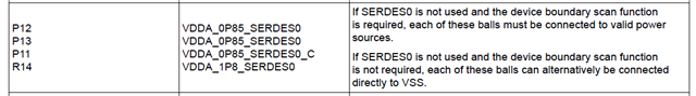
Connections to support Boundary scan 

JTAG connectors 

Let me know your thoughts.

  • Hi Board designers, 

    Refer below inputs for the JTAG connection related queries.

    https://software-dl.ti.com/ccs/esd/documents/xdsdebugprobes/emu_bsdl.html

    The AM625 (A53) run Linux.  What purpose is the JTAG used for in this processor?

     https://e2e.ti.com/support/processors-group/processors/f/processors-forum/1547247/am625-am625---jtag-custom-board 

    FAQs for reference related to JTAG, TRST, boundary scan, connector

    [FAQ] AM625: jtag schematics to implement in customer board
    e2e.ti.com/.../faq-am625-jtag-schematics-to-implement-in-customer-board
    e2e.ti.com/.../tda4vm-which-debug-signals-are-required-in-mass-production

    AM625: JTAG TRST signal pull down.
    e2e.ti.com/.../am625-jtag-trst-signal-pull-down
    AM623: AM6232ATCGGAALW JTAG Boundary Scan
    e2e.ti.com/.../5011656
    AM623: AM623, 10-pin JTAG adaptor and TRSTN
    e2e.ti.com/.../am623-am623-10-pin-jtag-adaptor-and-trstn 

    AM625: nTRST pin pulled low

    (+) AM625: nTRST pin pulled low - Processors forum - Processors - TI E2E support forums


    JTAG - pull resistor requirements
    Do TMS, TCK, TDI and TDO need a pull-up?
    Minimum recommendation is pull down resistor on TRSTn, pull-up resistor on TCK, TMS, and TDI. A pull resistor on TDO is optional.

    About JTAG signals
    The internal PU/PD of the JTAG signals ON state even during a reset, and it is possible to keep the internal PU/PD ON state even after a reset, but if system does not use JTAG feature, does JTAG siginals need to connect to external PU/PD ?

    Customers may think that the internal PU/PD is sufficient for signals processing, but customer want to confirm as double-check.
    The customer also connects the TRST pin to an external PD. The purpose is to ensure that the TAP controller is stopped. Is there any problem in processing this?

    The internal pulls are turned on by default during and after reset. They will remain on as long as software doesn't turn them off.
    External pulls are recommended anytime PCB traces are connected to the JTAG pins. The internal pulls are weak and they are not true linear resistors. They get weaker as the voltage approaches the voltage rail the resistor is pulling toward. Therefore, the internal pulls may not be able to hold signals in a valid logic state when external noise sources couple into the PCB signal traces.
    The external pulls should be connected to the same power rail as the internal pulls. For example, the EMU[1:0], TCK, TDI, TDO, and TMS pins are pulled to VDDSHV_MCU and the TRSTn pin is pulled to VSS.
    The customer should consider inserting a low pass filter on the TRSTn signal near the AM62Px pin, by inserting a 100 series resistor on TRSTn signal with a 0.1uF shunt capacitor on the processor side of the series resistor. I have seen external noise events couple into the TRSTn signal and creating random resets of the TAP controller while operating a debugger. This low pass filter will block transient noise events that cause unexpected resets to the TAP controller."
    "Customer wants to double check.

    Is the below understanding correct ?
    If system does NOT use JTAG, i.e. PCB traces are NOT connected to the JTAG pins, the internal PD/PU can be used.
    So , external PD/PU is NOT required when JTAG is not used.
    If system uses JTAG, i.e. PCB traces are connected to the JTAG pin, the external PD/PU should be used.

    That is correct. However, they would never be able to connect a debugger to the device if they do not connect PCB traces to JTAG."


    Boundary scan for AM62

    Please refer to Debug Boot Modes and Boundary Scan Compliance section (13.3.4) in the AM62x TRM.
    The boundary scan tool must set the EMU pins to the appropriate value before the rising edge of TRSTn to select the boundary scan TAP controller.

    Boundary Scan
    This device supports boundary scan using an IEEE 1149.1 compliant JTAG TAP that is made visible through the
    use of a compliance-enable mode (see Section 13.3.4). IEEE 1149.1 and 1149.6 Boundary Scan support are
    defined in device-specific BSDL files that can be found in the respective device’s product folder on ti.com.


    SoC Address Space
    The device architecture provides access to On-Chip debug resources through the SoC Address Space. This
    includes access to all DAP Access Ports (APs) as well as the Debug-APB address space.


    13.3.4 Debug Boot Modes and Boundary Scan Compliance
    The EMU1 and EMU0 device pins are used to convey debug boot mode behavior and can also be used as part
    of a boundary scan compliance sequence to enable boundary scan features.


    Debug & pins for connector

    Concerning debugging, it's not very clear in the documentation, for the JTAG and TRACE, are the 2 used for ARM and DSP?
    The number of pins required is significant, on the eval board it's a 60-pin connector, but they're not all used, so we can optimize, but even then it's still a lot of pins, aren't there any optional signals? Do we have to have everything? What surprises me is that some signals can be output on 2 different pins (table 6-115 of the datasheet).
    Regards

    JTAG signals (TRSTn, TCK, TMI, TDO, TDI) can be used to access any processing core within the device (includes ARMs and DSPs). You can access all registers, internal memory, etc. Standard debugger functionality. TRACE is used to collect information captured/logged by the processing core and off-loaded to external debugger for history, inspection, etc. Signals include CLK, CTL, and configurable data widths based on needed bandwidth. TRACE is an optional interface, but it is recommended to support JTAG as a minimum for debug.
    Our EVM uses MIPI-60 connector for JTAG + TRACE. There are other connector standards for mating with debuggers which have only JTAG and thus fewer pins.

    Regards,

    Sreenivasa

  • Hi Board designers, 

    Additional inputs for AM64x

    AM2434: How to do boundary scan testing
    e2e.ti.com/.../5165506

    For JTAG connector, TRST and TCK should pull up or pull down?

    The AM62x TRSTn signal should have an external pull-down on it and the other JTAG signals should have external pull-ups on them, including the EMU[1:0] pins. This prevents the JTAG pins from floating when a debugger is not connected.

    https://e2e.ti.com/support/processors-group/processors/f/processors-forum/1396794/am6442-for-jtag-connector-trst-and-tck-should-pull-up-or-pull-down/5345412


    The IEEE 1149 specification recommends pull-ups on all of the JTAG signals. However, TI doesn't follow that recommendation for TRST. We recommend TRST to be pulled low to hold the JTAG TAP controller in reset during normal operation to prevent any chance of noise generating conditions that cause the debug or boundary scan functions to do something unexpected. The only side-effect associated with not following the IEEE 1149 recommendation is some debuggers may need to be configured to operate their TRST output in push-pull mode if they default to open-drain mode. The debugger TRST output needs to operate in push-pull mode so it can drive the TRST signal high.
    Thanks for the clarify, what about TCK?
    A pull-up, as recommended by the IEEE 1149 standard.

    Regards,

    Sreenivasa

  • Hi Board designers, 

    Additional inputs for Boundary Scan 

    AM625: Availability of Boundary Scan if JTAG is locked
    we assume, that the boundary scan feature is NOT available if JTAG is locked in terms of security. On the other hand, if we unlock a previously locked device by, e.g., injecting a debug-certificate, boundary scan would be available again, too.
    Are those assumptions correct?
    Boundary scan functionality remains available for use, however downstream debug features that are typically available via JTAG are locked out.


    Boundary scan on HS-SE and TI-dummy key hardware TDA4VM
    With the JTAG locked down on TI-dummy key hardware and HS-SE hardware variants, is boundary scan functionality also included in the JTAG lock down? If the answer is no, what would TI recommend be the factory process for performing boundary scan with these hardware variants? (for the sake of this question, it can be assumed that the HS-FS component has had the eFuses blown to make it an HS-SE before boundary scan is run)
    Boundary scan is *not* locked on HS devices.

    Please confirm if Boundary Scan is possible for HS-SE device( without unlocking JTAG ) at manufacturing.
    Yes, BSCAN can still be used.

    We want to define the power up sequence for the boundary scan test on the TDA4VM.
    We were wondering if we should power up the board from the input power such that the PMICs can enable the various rails
    or should we apply voltages to the various rails through the test points? Or are there other methods to do the boundary scan?
    The power levels and sequence requirements for the standard operating mode and the boundary scan test are the same.
    No change in voltage levels for each power rail, no change in power sequence, and no change in which rails are required to be powered.

    https://e2e.ti.com/support/processors-group/processors/f/processors-forum/842779/am6548-boundary-scan/3116756?tisearch=e2e-sitesearch&keymatch=SPI0_CLK#3116756

    I'm looking for a list of AM6548 pins which are accessible over the boundary scan interface. This will helps me a lot to reduce the number of test points on the pcb for the purpose of ICT testing during the production. 

    The boundary scan model at SPRM724 can be used as an input to a script that extracts the information you're looking for. The "port" list will say "linkage" for pins that don't have a boundary scan cell and it will say "inout" for those that do. Here is the result of something I put together quickly, it can be used in excel or however you wish. There is more information in the boundary scan model that I did not extract, such as whether the pin is open-drain versus push-pull.

    RSV2 AA6 linkage
    RSV3 B1 linkage
    RSV4 AC23 linkage
    CSI0_RXN0 G28 linkage
    CSI0_RXN1 H27 linkage
    CSI0_RXN2 F26 linkage
    CSI0_RXN3 H25 linkage
    CSI0_RXN4 G24 linkage
    CSI0_RXP0 F28 linkage
    CSI0_RXP1 G27 linkage
    CSI0_RXP2 G26 linkage
    CSI0_RXP3 G25 linkage
    CSI0_RXP4 F24 linkage
    DDR_AC0 A10 inout
    DDR_AC1 D9 inout
    DDR_AC10 E7 inout
    DDR_AC11 A6 inout
    DDR_AC12 F7 inout
    DDR_AC13 D6 inout

    The signals listed in the BSM do reflect what is hooked up on the scan chain. Looking in the file one can pull out signals used in the DDR interfaces (and others) and see they are linked into the chain. If you know what interfaces you are using it should be possible to see if your usage needs are covered.For the tool level check I ran in this area, I only checked a few signals which I could observe on the EVM and saw it working as expected. Larger internal usage/testing does happen especially for chip level automated tests. I assume you are looking at this for board-level verification. For a given design a detail level check will be necessary. I assume there was a goal to cover as much as possible but that usually does not end up being every possible permutation. Are you at a point where don't know what all signals your design is using or are you looking to protect for future options? In our inspection so far did you find anything which was missing?

    A couple of quick follow up points:

    #1 The IOs in the bsm file listed as non-linkage are on the chain. The linkage ones are not scannable. I suspect you know this but its good to state it.

    #2 I did receive some comments from the designer who implemented the logic. He mentioned that the chain requirements were shaped based on test board requirements along with the characteristics of a given IOs logic. For a few complex IOs like PCIE there was not a path for scan inclusion.  Largely most IOs are covered. Looking in the BSM/BSDL file at the details as I have indicated will be part of your planning.

    AM2431: What does this boundary scan function refers to
    e2e.ti.com/.../am2431-what-does-this-boundary-scan-function-refers-to

    Boundary Scan
    e2e.ti.com/.../am623-jtag---boundary-scan

    AM6548: Boundary scan for HSFS on AM65x
    e2e.ti.com/.../am6548-boundary-scan-for-hsfs-on-am65x

    JTAG Boundary Scan functions should work the same way irrelevant of device types (GP or HS) i,e, JTAG Boundary Scan should always work. On the other hand, JTAG Debug Access depends on device types (GP or HS)

    e2e.ti.com/.../am625-boundary-scan-issues
    AM625: Boundary scan issues

    AM623: If CSI is not used but boundary scan is what to do with W13, W14?
    e2e.ti.com/.../am623-if-csi-is-not-used-but-boundary-scan-is-what-to-do-with-a8-and-a10

    AM62P5-Q1: Z1: HW: JTAG boundary scan on HS devices
    e2e.ti.com/.../am62p5-q1-z1-hw-jtag-boundary-scan-on-hs-devices

    AM2434: JTAG boundary scan and debug info/capabilities
    e2e.ti.com/.../am2434-jtag-boundary-scan-and-debug-info-capabilities

    Regards,

    Sreenivasa

  • Hi Board designers, 

    Additional inputs for EMU0/EMU1 Connections

    AM62A3-Q1: HW: When not using the JTAG port

    If JTAG is not used, is it OK to leave EMU0/EMU1/TCK/TDI/TMS/TDO/TRSTn open?

    Are you connecting any PCB traces to these pins? If so, they need external pull resistors to help hold a valid logic state. If not, you can leave them unconnected. However, this is very risky as you will never be able to connect a debugger to find what is happening if your system has problems.

    No PCB traces.TRSTn uses internal pull-down, other uses internal pull-up to open the balls.
    This is OK?

    Yes, as long as you do not connect any PCB trace to these package terminals.
    We expect external pulls to hold a valid logic state on these pins when any PCB trace is connected because the
    internal pull resistors are weak and non-linear. We make this recommendation because electrical noise could couple on the un-driven
    PCB traces and the internal weak pull resistor may not be able to hold a valid logic state. The internal resistor should be able
    to hold a valid logic state if no signal trace is connected to the terminals.
    This topic is addressed in the datasheet "Connectivity Requirements table.

    AM62] EMU0 / EMU1 with JTAG
    Could you tell us what additional features/data are availables whilst using the EMU0 and EMU1 in addition to the Normal JTAG ?
    The emu0/1 signals have 2 purposes. One is to control the device behavior upon booting; please refer to the AM62 TRM, section 13.3.4.
    The other adds cross-triggering capabilities for real-time debug purposes; please refer to the TRM section 13.3.6.


    TDA4AL-Q1: Are EMU0/EMU1 pins essential for On-chip Debug?

    Are EMU0/EMU1 pins essential for debugging a TDA4AL HS system using CCS/XDS560v2?
    These pins seem to optional according to some articles available on the Internet.
    Could we safely block these pins so that these pins are not connected to the emulator?
    (There are some limitations on the routing traces of the next board iteration, so it is desirable not expose EMU0/EMU1)

    EMU0, EMU1 can be used to halt the processor prior to ROM execution.
    This is sometimes important if debugging security issues, as that can impact access to the device via JTAG. If needed to debug initial boot/security issues - then I would recommend supporting. If debug efforts are beyond that (more application/peripheral level) then may not be needed.

    As per your reply, typical R5 SBL and boot app debugging sessions have nothing to do with the EMU0, EMU1 pins?

    The EMU0/EMU1 pins are not JTAG and are not part of the TRACE logging interface (TRC).
    They are available in the Debug IP can be setup for generic triggers.


    TDA4VM-Q1: BSDL test point
    Our customer is preparing do BSDL test and find they don't place test point on EMU1. Which part of test coverage will drop if BSDL is not tested? Do we have the document/guide to elaborate the hardware configuration of Jacinto BSDL test?
    On TDA4VM (J7ES) it is required to have EMU1=0 at POR to enter BSDL mode. They will not have access to boundary scan if this is not available.
    The public BSDL file for TDA4VM is here www.ti.com/.../sprm751
    It gives details of what pads are on the chain. Its compliance pattern does call out EMU1=0 for mode entry.
    attribute COMPLIANCE_PATTERNS of J721E : entity is "(ddr_ret, porz, mcu_porz, reset_reqz, mcu_resetz, emu0, emu1)(0111110)";

    There are several domains and multiple function modules in the SoC. Customer would to like to know which parts that BSDL test can cover?
    Customer want to evaluate the impact if they cannot run the BSDL test.
    Production chips on a customer board will only be able to test the actual IOs on the scan chain.
    Some customers use this to look for open/shorts on the PCB, additionally some use BSDL as a backup way to bit-bang burn a flash chip on a board.

    TDA4AH-Q1: usage of EMU[1:0] TI extensions

    what is the usage of the EMU[1:0] TI extensions lines? On our board we have no possibility to connect them to the JTAC . We plan to connect them to a fixed level via resistor. From the EVM page 4514 it seems that connecting both to high is a good idea? What will we lose with having no connection to a connector?

    Both EMU0 and EMU1 should be pulled high via a 1K-ohm to 10K-ohm resistor for default settings/productions systems.
    EMU0/1 on DEV systems should be exposed and settable. They get used to:

    Signal BSDL mode entry (POR latched) used for open/short testing and possible flashing
    Signal WIR mode entry (POR latched) which can be used to run bare metal code used with char projects
    Without this a working firmware and basic boot image have to be golden.
    This can be a chicken and an egg for a new board.
    WIR also allows initial flash burning on an HS boards using JTAG
    The alternate is to ensure a UART boot is possible + a stable boot image + stable flasher in that boot image.
    The above can have lots of detail issues which a JTAG burn totally bypasses
    Run time external trigger sources used in conjunction with debugger and external devices
    Run time (non-por related)

    MCU-PLUS-SDK-AM243X: hardware JTAG debug emu0 emu1
    e2e.ti.com/.../mcu-plus-sdk-am243x-hardware-jtag-debug-emu0-emu1

    EMU0/1 is useful externally for:
    Wait-in-Reset (WIR)
    Useful on HS devices for early board checkout and JTAG flashing
    Boundary Scan
    Useful for old style open/short testing and flashing burning
    Debug-Triggers
    Can be input our output triggers linked to different debug actions

    Therefore, we encourage you to connect the EMU[1:0] pins to the debug connector and use external pull-ups to hold these signals high when not connected to a debugger.

    e2e.ti.com/.../5043123

    e2e.ti.com/.../4424403
    AM2434: In JTAG debugging, how can I connect EMU0 and EMU1?

    e2e.ti.com/.../am625-am6254x-emu0-emu1
    AM625: AM6254X EMU0 EMU1


    e2e.ti.com/.../sk-am62a-lp-am62a-series-mpu-jtag-connection
    SK-AM62A-LP: AM62A series MPU JTAG connection

    The level-translators were used to prevent a potential from being applied to device pins when the device IO power rails are turned off while the on-board debugger is still powered. Please refer to the "Steady-state max voltage at all fail-safe IO pins" parameter in the datasheet Absolute Maximum Ratings table.

    All paths through the SN74AVC8T245R device you proposed must flow in the same direction at any one time. There is no way to configure the TDO signal path to flow from the SOC to the connector while the other signals are flowing from connector to the SOC. All SOC signals must be connected to the A port and all connector signals must connect to the B port since the A port is powered by the same IO supply as the SOC signals and the B port is powered by the same IO supply as the connector signals.

    I do not know why the PCB designer used a TXS0102D to level-shift the EMU[1:0] signals. I would need to assign this thread to someone from the hardware design team if you need to know why this device was used for the EMU signals. 

    Are you designing a production PCB?  If so, why are you implementing the on-board XDS110? Most customers only place a JTAG connector on their production PCB to avoid the additional cost of the on-board XDS110 components and they connect an external debugger to the PCB when it is needed to debug an issue. We included the on-board debugger to make it easy for customers to begin development.


    The JTAG connector sources power to the debugger because it has an internal level-shifter with its SOC port powered from the target. The buffer/level-shifter components in each JTAG signal path are also operating like a switch to select between the on-board debugger or the connector. Most customers place the connector within a few inches of the processor and connect the pins directly to the SOC, with the appropriate external pull resistors.

    The signal trace length of 6 inches is not a firm requirement. Short signal traces will minimize signal distortion and signal propagation delay. The most important thing is making sure the clock signal doesn't have any non-monotonic transitions. You can always resolve timing issues by slowing down the operating frequency of TCK from the debugger.

    e2e.ti.com/.../5043123
    AM62A7: AM62A AXI bus access doesn't show anything
    The solution was to use WIR mode to get near GP accessibility. To get this state EMU0=0 and EMU1=1 needs to be driven. With that configuration now registers are accessible.

    e2e.ti.com/.../5031751
    TDA4VH-Q1: Debugger Header options

    Regards,

    Sreenivasa

  • Hi Board designers, 

    Additional inputs for bootmode configuration latching.

    Customer Query: AM2432 Configure the Boot Mode After Powerup

    I am working on AM243x-EVM. I tried to load the firmware in DEV mode in powerup.

    After the loading by JATG, I tried to switch the boot mode to DFU mode (by configure the boot mode switcher) to make the USB port can be recognized by my application.

    But it did not work.I would like to know if this method recommended. Please suggest if there is any tip to implement this. 

    Suggested reply:

    This is not the recommended or expected way to configure the boot and may not work. To configure the Boot mode to DFU, the bootmode is required to be configured before the board is powered-up.  

    This is the reason MCU+SDK also recommends to POWER-OFF the EVM, change the bootmode pins setting to configurethe required bootmode and then POWER-UP the EVM.

    Since the application has been loaded using JTAG, there is no need for the DFU boot anyways.

    If you want USB DFU support in your application then you make use of USB SW stack available in the MCU+SDK: https://software-dl.ti.com/mcu-plus-sdk/esd/AM243X/10_01_00_32/exports/docs/api_guide_am243x/USB_DEVICE_DRIVER.html

    There is also an example application available on USB DFU: https://software-dl.ti.com/mcu-plus-sdk/esd/AM243X/10_01_00_32/exports/docs/api_guide_am243x/EXAMPLES_USB_DFU.html

    FYI, TRM reference for AM64x

    4.2.3 Boot Process Flow

    The values of BOOTMODE[15:0] pins are latched into the Device Status register
    CTRLMMR_MAIN_DEVSTAT[15:0] by hardware as the device comes out of global cold reset, sampled after
    MCU_PORz deassertion.

    (+) AM2432: AM2432 Reset by JTAG TRSTn - Arm-based microcontrollers forum - Arm-based microcontrollers - TI E2E support forums

    Let me try to add some additional information with respect to your question about using an external circuit that ensures the appropriate BOOTMODE value is presented to the AM243x device when the MCU_PORz signal rises. There may be cases where the pins associated with the BOOTMODE inputs are being used in a system that implements a specific peripheral via the same pins after the device has booted. In some of these cases, it may be necessary to implement an external circuit that blocks or isolates the effect of the other devices attached to these pins when the BOOTMODE inputs need to be a specific value to select a boot mode. Therefore, it may be necessary to implement a circuit that isolates or over-drives any conflicting pulls associated with attached devices.

     [FAQ] AM625 / AM623 / AM620-Q1 / AM64x / AM243x / AM62Ax / AM62Px / AM62D-Q1 / AM62L - Bootmode implementation with isolation buffers used

    Regards,

    Sreenivasa

    Regards,

    Sreenivasa

  • Hi Board designers, 

    Additional information for enabling boundary scan using  EMU0..1

    The BSDL model (bsm) found online does not work

    Can you please confirm if you have changed the logic states applied to the EMU[1:0] inputs to place the device in boundary scan mode?  

    Refer Below and TRM for more information.

    Regards,

    Sreenivasa

  • Hi Board designers, 

    I have the below question from a customer.
    Either case. AM243x can be warm reset from JTAG interface or JTAG connector?
    I looked at the debug chapter and do not see an option to reset the SOC through JTAG interface. Any thoughts please.

    Expert 1:

    JTAG interface does perform a warm reset using the System Reset menu selection. You could also perform a reset by writing to one of the Control Module registers which perform software resets. There is also a EMU_RESET signal on some JTAG headers which could be implemented as a cold/warm reset by toggling it from the emulation software, but it requires proper connection on the board and only certain JTAG emulators support this feature.

    Expert 2: 

    I agree the 20-pin JTAG connector defines two reset pins, one is named TRSTn and the other is named /RESET. The TRSTn signal is the one that must be connected to the JTAG peripheral to reset the JTAG TAP controller. The /RESET signal is an optional output from the debugger that can be implemented as needed by the customer. It can be connected such that it resets the entire system, or a portion of the system. It can be connected such that it creates a power-on reset to our device, or a warm reset to our device. So the action taken from the debugger depends on how the customer connects the /RESET signal as a reset source.

    I have been seeing a lot of customers trying to implement the 10-pin JTAG connector defined by ARM. This connector does not have the TRSTn signal or the EMU[1:0] signals. We need to make it very clear we expect customers to use the TI defined 20-pin connector rather then the 10-pin ARM connector.

    JTAG
    e2e.ti.com/.../5727433
    https://e2e.ti.com/support/processors-group/processors/f/processors-forum/1481150/dra821u-q1-can-dar821u-q1-bootup-from-jtga/5688673?tisearch=e2e-sitesearch&keymatch=JTAG%20%2Freset#5688673

    AM3358: Connect JTAG after entering Linux

    (+) AM3358: Connect JTAG after entering Linux - Processors forum - Processors - TI E2E support forums

    Regards,

    Sreenivasa

  • Hi Board designers, 

    Refer below information:

    I want to study the role of JTAG in AM625 processor ,actually how it operates ? 

    https://e2e.ti.com/support/processors-group/processors/f/processors-forum/1354325/processor-sdk-am62x-what-is-the-role-of-jtag-in-am625-processor-what-are-the-dependancy-of-jtag-in-am625/5165620

    In one mode the JTAG peripheral provides a way to communicate with the debug subsystem TAP controller, where you can use a debugger and its software to control and trace codes execution. In another mode the JTAG peripheral provides a way to communicate with the boundary scan TAP controller, where you can use a different set of tools to scan test patterns into and out of the device pins to perform board level testing.

    I'm not familiar with the various tools required to utilize these features, so I'm not able to answer any questions related the capabilities or usage of these tools.

    You will need to research what is provided by the various tool vendors and discuss capabilities with them.

    https://e2e.ti.com/support/processors-group/processors/f/processors-forum/1318078/am623-am6232atcggaalw-jtag-boundary-scan/5011656#5011656

    AM62x provides boundary scan as long as you apply power to all of the device power rails. I mention this because there is an option for not applying power to CSI0_TX if not used, but this will break the boundary scan path inside the device. See the Connectivity Requirements table in the datasheet.

    The logic state of the EMU[1:0] inputs are sampled on the rising edge of TRSTn to determine which TAP controller is selected. Please refer to the On-Chip Debug section found in the device TRM for more information.

    You will need to submit the Ethernet PHY question on an E2E forum associated with the device in question, so the appropriate team can answer your questions.

    You should be able to connect the JTAG ports in a daisy chain if the IO voltages are compatible and this connection topology doesn't cause any power sequencing issues. This means the JTAG ports and the Ethernet ports of both devices need to receive power from the same IO supply, so they sequence on/off at the same time. Note: the AM62x IOs are not fail-safe and I suspect the same is true for the Ethernet device.

    e2e.ti.com/.../am62a7-10-pin-jtag-connector-support

    Please find the answers to your questions after internal discussion with our JTAG expert:

    Due to limited space on a custom board, we would like to implement a 10-pin ARM Cortex JTAG header to do JTAG debugging of the AM62A7. Is this possible? I understand that we would lose TRACE and EMU support, but we don't plan to use those anyways. 
    I read this forum post and was wondering if this is true for our processor. If we can't use the 10-pin JTAG connector because of the TRST requirement, what would the next smallest JTAG connector be?
    XDS110 Debug Probe
    For debug probes, we were considering the XDS110 with a 20-pin to 10-pin adapter. Would a standard SEGGER J-Link debugger with a 10-pin connection such as this one also work? 

    Regards,

    Sreenivasa

  • Hi Board designers, 

    Refer below information relate to JTAG pulls.

    Customer Query:

    The customer is considering the following configurations:

    • NTRST, TDI, TDO, TMS: 10kohm pull-up
    • TCK: 10kohm pull-down

    Is this no problem?

    We expect nTRST to be pulled down and  all other JTAG interface signals (everything else) to be pulled up.

    Make sure they do not forget to put external pull-up resistors on the EMU[1:0] signals.

     We have seen cases where nearby ESD events can couple into the nTRST signal and cause the unexpected resets.  This can happen when the debugger has a long unshielded cable.  Therefore, they should consider putting a low-pass filter in the nTRST signal path.  In the past we have used a 100 ohm series resistor and 0.1uF shunt capacitor on the processor side of the series resistor to help resolve this issue.

    The recommendations are same for AM335x, AM437x, AM64x, AM234x (ALV, ALX), AM62A, AM62P, AM62L family of processors.

    Regards,

    Sreenivasa

  • Hi Board designers, 

    Refer below information related to RTCK.

    https://e2e.ti.com/support/processors-group/processors/f/processors-forum/1463952/tms320c6416t-request-for-length-matching-details---tms320c6416tbclzd1/5630349

    We are referring the below document for the layout guidelines for JTAG interface of DSP part TMS320C6416TBCLZD1.  

    Document URL: www.ti.com/lit/ug/spru641/spru641.pdf?ts=1737350351360&ref_url=https%253A%252F%252Fwww.google.com%252F

    Do we need to length match return signal path of TCK with the path of actual TCK? Please refer the below image for return signal path of TCK.

    The JTAG peripheral changes signals on the falling edge of TCK and latch signals on the rising edge of TCK. Therefore, you can always resolve any setup time or hold time violations by reducing the frequency of TCK. This eliminates any need to limit or match trace delays as long as you are willing to reduce the operating frequency of the JTAG peripheral. 

    Some debuggers can be configured to use RTCK as the capture clock for the TDO signal, as a way to compensate for round trip PCB and cable delays. This may allow the JTAG peripheral to operate at a higher frequency. The real benefit is when the target device has a RTC output signal that also compensates for the delay introduced by the target device. The TMS320C6416 device doesn't provide the RTCK output, so one option is looping the TCK signal back to debugger. However, this option can be problematic. The debugger may support a configuration option that uses its own TCK signal as the TDO capture clock rather than the looped back TCK signal. If so, this may be a more reliable option because branching the TCK signal into two paths on the target PCB can introduce signal integrity issues on the TCK signal. It is very important that your PCB design doesn't introduce any signal distortion on the TMS320C6416 TCK input such that it sees non-monotonic transitions. You should simulate signal distortion introduced by your PCB design to confirm your design is robust if you loop the TCK signal back to RTCK.

    Thanks for your replies and request you to provide us below inputs as well.

    1. Are there any reference layout files with looped back TCK RET signal?

    2. Whether TCK RET signal is compulsory to program TMS320C6416T DSP or TCK RET is just for increasing the speed of programming?

    3. At which point in the trace of actual TCK, we need take looped back RET TCK signal?

    This device pre-dates my support, so I'm not familiar with any PCB layout references. Use the method described in my answer to #3.

    As mentioned in my previous reply, RTCK support may be optional for some debuggers. The RTCK signal was implemented to improve operating speed of the JTAG peripheral, but it may not be required for some debuggers. You will need to ask the debugger manufacture if the RTCK is required for their debugger to operate properly. It is not required by the TMS320C6416 device.

    The buffer shown in the schematic snapshot inserted above would need to be placed very close to the TMS320C6416 TCK input pin such that each leg of the signal trace branch is very short and equal length (a short-T clocking topology). You should also include a pull-up on the TCK signal to ensure it is not floating when a debugger is not connected.

    AM62A7-Q1: Multiple devices in JTAG scan chain
    www.ti.com/.../spru655i.pdf
    If there is additional insight regarding 2xAM62D's in the same JTAG scan chain, please pass along. For example, CCS/Emu support, further HW considerations, etc.

    There is some information in the below document: dev.ti.com/.../node
    See the section on "multiple devices". However, I think the information above may be a subset of what is already in the document you referenced.
    As for information specific to multiple AM62s, I don't have any experience myself. Perhaps the device experts can share more information.

    I'm not aware of anyone that has tried to connect two AM62Ax devices in the same JTAG scan chain. There should not be any hardware issue with connecting two in the same chain as long as the IOs associated with JTAG pins of both devices are powered from the same source. The IOs implemented in the AM62Ax devices are not fail-safe, so you must ensure no potential is applied to any of the IOs until the respective IO power rail is valid.

    In our project, I'm also interested in this JTAG chain mode. From your reply, I think the HW can support the JTAG chain mode as long as it can meet some known HW rule. We can refer to the link :dev.ti.com/.../node
    However, if we want to use the JTAG chain, we have to require that the Software IDE/CCS also can support it. How about your opinion/experience about it?

    Ki is from the team that supports the software development tools. I can only answer questions related to electrical and timing requirements and characteristics of the JTAG peripheral. I do not know anything about how the software debug tools communicates with internal debug subsystem.

    However, if we want to use the JTAG chain, we have to require that the Software IDE/CCS also can support it. How about your opinion/experience about it?
    Code Composer Studio comes with all the necessary software/drivers for our XDS JTAG based debug probes.

    I checked the link:www.ti.com/.../spru655i.pdf and XDS JTAG based debug probes.
    It looks the 10pin connector will not support JTAG chain, is it right?
    And the RTCK signal is necessary. However, I didn't find the RTCK pin in AM62D and AM62A. Do you know how to deal with it?

    I'm not familiar with a 10-pin connector option. The document referenced in your previous reply describes a 14-pin, 20-pin, and 60-pin connector options. The document also tells you to connect RTCK to either a loopback of the emulation header's TCK or a target device-supplied RTCK. The AM62Ax devices do not implement a pin to source the RTCK signal, so you must loopback the TCK signal.

    https://e2e.ti.com/support/processors-group/processors/f/processors-forum/1427556/tda4ve-q1-jtag-pin-map-query/5480938


     Q.) What is the purpose and function of EMU0, EMU1
    EMU0, EMU1 are signals used to put processor in special test modes, and are typically not required for most developers.

    Is it mandatory that RTCK should be connected to TCK?

    I know if the JTAG target(TDA4VE) doesn't have RTCK port, we don't need to connect RTCK.

    The reason why I asked, If we connect RTCK with TCK, our system may have long T-branch connection.

    So if It is not mandatory, I don't want to connect it.

    RTCK should be connected to TCK. See TI's EVM as an example of this.

    RTCK requirement would be emulator dependent. As you stated, its not supported on the TDA4VE. It only needs to be connected if required by the connected emulator.

    https://e2e.ti.com/support/microcontrollers/arm-based-microcontrollers-group/arm-based-microcontrollers/f/arm-based-microcontrollers-forum/1349818/am2431-regarding-jtag-queries/5158725 

    We are designing a custom board using AM2431
    We refer to EVM circuit which is attached . In that pdf page no 23 JTAG section
    We have some quires which We like to know things below
    1. How 20 pin connector support JTAG and Emulator function
    2. As we the requirement we don't have space for multiple device, So we are planning to remove the buffer . Does it cost any issue (as reference as block diagram)
    3. RTCK loopback ,Do we need to add buffer in between
    PROC101C(005)_SCH (1) 4.pdf

    The buffers inserted in the TMS, TDI, TDO, and TRST signal paths are being used as level shifters to ensure the debugger does not applying any potential to the AM243x pins when the debugger is connected, and power is turned off to the AM243x device. The AM243x pins are not fail-safe, so your system implementation must never apply any potential to the AM243x pins when it is not powered. See the "Steady-state max voltage at all other IO pins" parameter in the Absolute Maximum Ratings table found in the AM243x datasheet.

    The buffers in the TCK and RTCK paths provide the same voltage level translation function as well as preserving signal quality of the debugger clock source that needs to branch into to two paths, where one path sources the AM243x device and the other path returns a delayed clock to the debugger to improve timing margin at high operating speeds.

    Your debugger may not require a RTCK. If so, you may not need to branch the debugger clock source.

    Some debuggers have an internal level translator, where the same AM243x IO power source is routed to the JTAG header and powers the downstream side of the level translator in the debugger. If so, you may not need the level translators.

    You need to understand these types of details associated with the debugger you plan to attach and design your system to accommodate the requirements of both AM243x and the debugger under all possible use cases. This is the system designer's responsibility.

    Thank you for the response. We are using XDS110 debugger for custom design
    Can we proceed with this debugger with our custom design.

    Yes, you should be able to use the XDS110 debugger.

    https://e2e.ti.com/support/processors-group/processors/f/processors-forum/1164867/faq-am625-jtag-schematics-to-implement-in-customer-board/4381563#4381563

    They should connect TMS, TDI, TDO, TCK, EMU0, and EMU1 from the connector directly to the AM62x device with separate external pull-ups on each of these signals.

    They should connect TRSTn from the connector directly to the AM62x device with an external pull-down on this signal.

    They will need to research the debugger expectation for the RTCK connection. Some debuggers may require a RTCK, while others have a configurable option to use it or ignore it. I have seen people simply loop TCK back to RTCK near the connector, but this can cause signal integrity issues. Splitting a signal trace like this can cause reflections that can introduce clock glitches. I suggest placing two resistors near the TCK connector pin and inserting one in series with the TCK signal connecting to the AM62x device and the other in series with the RTCK path when TCK is looped back to RTCK. This acts like series terminations and the resistor values can be adjusted to impedance match the signal transition into two paths which also attenuates any undesired reflections.

    The supply connected to the debugger connector should be the same supply that is connected to IO power rail of the AM62x JTAG IOs (VDDSHV_MCU).

    They should also reference the following document: Emulation and Trace Headers

    https://e2e.ti.com/support/processors-group/processors/f/processors-forum/1119621/tda4vm-tda4vm-jtag-wiring-problem-to-ask/4152008

    https://e2e.ti.com/support/microcontrollers/arm-based-microcontrollers-group/arm-based-microcontrollers/f/arm-based-microcontrollers-forum/1029515/faq-tms570lc4357-jtag-connection-issues-to-hercules-devices/3805893

    1. Is JTAG RTCK required for target connection?

      RTCK is not a standard JTAG signal. The asynchronous TAP controller does not require local synchronization, so the RTCK is not a MSUT.

      But, occasionally a target device requires the JTAG interface to be externally synchronized to a clock within the device due to it being slow, non-continuous, or variable. The adaptive clocking feature uses the RTCK to address this requirement. When adaptive clocking is enabled, the debug unit issues a TCK signal and waits for the RTCK signal to return before sampling TDO.

      If you emulator supports adaptive clock feature, and you are planning to use this feature, you need RTCK from the target device.

    2. What are the differences between JTAG and ETM?

      JTAG: The functionality usually offered by JTAG is Debug Access and Boundary Scan: 1. Debug Access is used by debugger tools (for example XDS110, XDS2x) to access the internals of a chip making its resources and functionality available and modifiable, e.g. registers, memories and the system state. 2. Boundary Scan is used by hardware test tools to test the physical connection of a device, e.g. on a PCB. This is usually not the task of a debugger tool.

      ETM: The Embedded Trace Macrocell (ETM) interface enables you to connect an external ETM unit (for example XDS560V2 Pro) to the processor for real-time code tracing of the core. JTAG signals are also required for ETM trace.

    1. Why should the nTRST signal be pulled LOW?

      nTRST is JTAG “Test Reset”. It is low active. The nTRST is used for an asynchronous reset of the state machine of the JTAG Test Access Port (TAP). The debugger drives it by a push-pull driver. It resets the TAP by a certain JTAG sequence. The target device requires that the nTRST is first held low for a few TCK cycles and then raised after the TCK signal has started running, so the device can detect a rising edge on nTRST.

      A pull-down resistor should be added onto nTRST on target side. It ensures the on-chip debug logic is inactive when the debugger is not connected.

      From the debugger point of view, nTRST is optional.

    1. The JTAG connection is lost after the program is loaded to flash.

      The problem might be caused by the code you have programmed. The code in the flash makes the CPU enter an exception state repeatedly, and the CPU is not able to enter a debug state.

      Please try this procedure to let CPU enter a debug state:

      1. Open the target configuration window, and launch the selected the configuration
      2. Switch to debug window.
      3. Press the reset (nRST) button and hold it.
      4. Click “Connect Target” immediately after you release the nRST button.
      5. The board should be connected after couple tries.

           5. Please refer to the following link for more information to trouble shoot the JTAG connection issues:

                 https://software-dl.ti.com/ccs/esd/documents/ccs_debugging_jtag_connectivity_issues.html

    Regards,

    Sreenivasa

  • Hi Board designers, 

    Queries related to lauterbach trace32 cmm files

    e2e.ti.com/.../5857553

    Regards,

    Sreenivasa

  • Hi Board designers, 

    Bootmode dependency for boundary scan

    The Boundary scan configuration after reset is a state machine controlled by the EMU0..1 pins.

    There is no dependency on the bootmode configuration to run the boundary scan testing.

    Regards,

    Sreenivasa

  • Hi Board Designer,

    Inputs regarding XDS560 and XDS110

    (+) AM62D-Q1: Using XDS560v2 with AM62D-Q1 - Processors forum - Processors - TI E2E support forums

    AM62D-Q1: Using XDS560v2 with AM62D-Q1

    You will need to connect the EMU[1:0] pins to the debugger if you have any plans to place the device into any of the modes defined by the tables inserted above. The debugger is also able to use the EMU[1:0] pins to signal trigger events between the AM62Dx debug subsystem and the debugger.

    I'm not sure what trace functions are currently supported by the TI Code Composer Studio (CCS) tools. I seem to recall hearing the CCS tools no longer support some of the trace functions, but that comment may be related to the trace functions associated with the trace port (TRC_CLK, TRC_CMD, and TRC_DATA signal functions). I will assign this thread to the CCS team and let them comment on what is supported by CCS and the XDS560v2 debugger.

    (+) AM620-Q1: TI-Debugger - Processors forum - Processors - TI E2E support forums

    (+) TMDSEMU560V2STM-U: User's guide or Tecnical Reference - Processors forum - Processors - TI E2E support forums

    The JTAG, EMU, and TRACE section of the AM62x datasheet provides a link to documents that define the connectivity requirements to various connectors.

    (+) AM623: JTAG - Boundary scan - Processors forum - Processors - TI E2E support forums

    (+) TMDSEMU560V2STM-UE: Need help for TMDSEMU560V2STM-UE installation procedure - Processors forum - Processors - TI E2E support forums

    (+) TMDSEMU560V2STM-UE: TMDSEMU560V2STM-UE: 3d cad model (stp or igs) and/or Pacakage outline needed - Processors forum - Processors - TI E2E support forums

    (+) TMDSEMU560V2STM-U: Cable Break Issue - Processors forum - Processors - TI E2E support forums

    (+) TMDSEMU560V2STM-U: Broken Flat Cable - Processors forum - Processors - TI E2E support forums

    (+) TMDSEMU560V2STM-U: TMDSEMU560V2STM-U USB Interface - Processors forum - Processors - TI E2E support forums

    (+) AM620-Q1: The XDS110 cannot connect to the M4F core and the R5 core - Processors forum - Processors - TI E2E support forums

    finally we verify the cause is TRSTN. when we connect XDS110 TRST_N to TDA4VE TRSTN, it works.

    Regards,

    Sreenivasa

  • Hi Board Designer,

    Inputs regarding boundary scan.

    A boundary scan test is mean to be a system level test that confirms connectivity between devices on a PCB assembly by validating pins which should be connected are actually connected and the signals that connect devices are not shorted to other signals. Therefore, you would not need to test any pins that are not normally connected in a valid system implementation. For example, you show the MCU_RESETSTATZ output and the MCU_RESETZ and RESET_REQZ inputs not connected in the snapshot inserted above. There would not be any value in testing these pins. Note: You would be required to add an external pull-up on the MCU_RESETZ and RESET_REQZ inputs if you attach any signal trace to the package pins associated with these inputs.  

    Boundary scan will only function after the device has all power rails powered and has been released from reset, which requires a valid reference clock from MCU_OSC0 for the synchronous release of reset to propagate from the MCU_PORz input to all internal circuits. The AM62x boundary scan doesn't touch the MCU_OSC0_XI and MCU_OSC0_XO pins. These pins must remain connected the same as they would be connected for normal system operation. 

    You must connect the TDI, TDO, TCK, TMS, TRSTn, and EMU[1:0] signals to a tool that performs the appropriate boundary scan function. We suggest connecting these signals to one of the commonly used JTAG headers (14-pin or 20-pin), where the TRSTn signal has an external pull-down and all of the other signals have an external pull-up. You would connect your boundary scan tool to this header. The EMU[1:0] inputs must be set to a specific logic state and latched on the rising edge to TRSTn for the device to enter boundary scan mode. Please refer to the TRM to find the appropriate logic state required on the EMU[1:0] inputs to enter boundary scan mode. Note: Any device package pin that has a signal trace connected is expected to have an external pull to hold a valid logic state. The weak internal pull should not be used to hold a floating signal trace in a valid logic state. External pulls are required on floating signal traces because the internal resistor may not be strong enough to hold a valid logic state when noise is coupled to the floating signal.

    Additional query

    Looking at BSDL file of AM62, the COMPLIANCE_PATTERNS attribute lists:

    attribute COMPLIANCE_PATTERNS of AM62 : entity is "(emu0, emu1, mcu_osc0_xi, mcu_porz, mcu_resetz, reset_reqz)(10X111)";


    That means these six pins must be in specific logic states ("10X111") during boundary‑scan tests to ensure proper operation

    If we dive into we get :

    emu1 low selects the correct TAP (Test Access Port) on the device.

        emu0 = 1, emu1 = 0 emu0 high, 

    mcu_osc0_xi is ignored by JTAG itself—likely irrelevant to boundary‑scan.

        mcu_osc0_xi = X (don’t-care) 

    mcu_porz, mcu_resetz, reset_reqz must all be de‑asserted (held inactive, high‑level) during boundary‑scan operations.

        mcu_porz = 1

        mcu_resetz = 1

        reset_reqz = 1

    As you noticed we not use the MCU in our application, but supplier argue that during BS operation even not using MCU it is mandatory to ensure proper state of these signals otherwise it will abort the BS process.MCU_PORz – MCU domain cold‑reset input. Must be high (inactive). If low, MCU domain stays in reset
    .

    MCU_RESETz – MCU domain warm/hot‑reset input. Must be high (inactive) to allow scanning.

    RESET_REQz – Main domain hot‑reset request. Must also be high (inactive) to not interfere.

    MCU_OSC0_XI – Clock input for MCU domain oscillator; boundary‑scan doesn’t depend on its state—labeled “don’t‑care”.

    So our understanding to correctly enter boundary‑scan mode and ensure proper compliance:

     emu0 = high, emu1 = low to route the JTAG TAP.

     Ensure MCU_PORz, MCU_RESETz, RESET_REQz are all de‑asserted (high) during the scan (not sure if TI can confirm if by default keeping those pins NC is enough or not).

    ️ Hold EMU pins stable—typically via pull‑ups/pull‑downs—and ensure reset signals are not floating or glitch-prone.

    I remain convinced that the oscillator input mcu_osc0_xi can be ignored for JTAG purposes.

    The BSDL may say mcu_osc0_xi = X (don’t-care), but the expectation is this pin and the mcu_osc0_xi pin is connected to one of the two valid clock sources described in the "MCU_OSC0 Internal Oscillator Clock Source" or "MCU_OSC0 LVCMOS Digital Clock Source" sections of the datasheet.

    You should not connect any signal trace to the package pins associated with the MCU_RESETz and RESET_REQz inputs because the device has internal pull-ups that will hold a logic high state on these inputs as long as you do not connect any signal traces that can act like antennas and pickup noise. These pull-ups are defined in the "BALL STATE DURING RESET RX/TX/PULL" and "BALL STATE AFTER RESET RX/TX/PULL" columns of the Pin Attributes table in the datasheet.

    The EMU[1:0] inputs are captured on the rising edge of TRSTn, so they only need to be held in the 0b01 state for a few ns after the rising edge of TRSTn to ensure there is no hold time violation.

    Regards,

    Sreenivasa

  • Hi Board Designer,

    Additional Inputs regarding boundary scan.

    We are going to evaluate the Boundary Scan coverage via JTAG port

    AM6202, BSCAN test mode require test points of JTAG interface (that we have already implemented) plus compliance signals that are currently missing (listed bellow).


    Grid Name

    Nail Number

    Pattern

    U5000 (AM6202 ALW)


    TDI

    A11

    171
    (From Golden Finger now, better have normal test point)

    1/0

    TDO

    D12

    172

    (From Golden Finger now, better have normal test point)

    1/0

    TCK

    A10

    170
    (From Golden Finger now, better have normal test point)

    1/0

    TMS

    B11

    173
    (From Golden Finger now, better have normal test point)

    1/0


    Compliance


    emu0

    E12

    168

    1

    emu1

    C11

    169

    0

    mcu_osc0_xi

    B2

    NP(No interface available currently)

    x

    mcu_porz

    D2

    NP (No interface available currently)

    1

    mcu_resetz

    E11

    NP (No interface available currently)

    1

    reset_reqz

    F20

    NP No interface available currently)

    1

    A boundary scan test is mean to be a system level test that confirms connectivity between devices on a PCB assembly by validating pins which should be connected are actually connected and the signals that connect devices are not shorted to other signals. Therefore, you would not need to test any pins that are not normally connected in a valid system implementation. For example, you show the MCU_RESETSTATZ output and the MCU_RESETZ and RESET_REQZ inputs not connected in the snapshot inserted above. There would not be any value in testing these pins. Note: You would be required to add an external pull-up on the MCU_RESETZ and RESET_REQZ inputs if you attach any signal trace to the package pins associated with these inputs.  

    Boundary scan will only function after the device has all power rails powered and has been released from reset, which requires a valid reference clock from MCU_OSC0 for the synchronous release of reset to propagate from the MCU_PORz input to all internal circuits. The AM62x boundary scan doesn't touch the MCU_OSC0_XI and MCU_OSC0_XO pins. These pins must remain connected the same as they would be connected for normal system operation. 

    You must connect the TDI, TDO, TCK, TMS, TRSTn, and EMU[1:0] signals to a tool that performs the appropriate boundary scan function. We suggest connecting these signals to one of the commonly used JTAG headers (14-pin or 20-pin), where the TRSTn signal has an external pull-down and all of the other signals have an external pull-up. You would connect your boundary scan tool to this header. The EMU[1:0] inputs must be set to a specific logic state and latched on the rising edge to TRSTn for the device to enter boundary scan mode. Please refer to the TRM to find the appropriate logic state required on the EMU[1:0] inputs to enter boundary scan mode. Note: Any device package pin that has a signal trace connected is expected to have an external pull to hold a valid logic state. The weak internal pull should not be used to hold a floating signal trace in a valid logic state. External pulls are required on floating signal traces because the internal resistor may not be strong enough to hold a valid logic state when noise is coupled to the floating signal.

    The BSDL may say mcu_osc0_xi = X (don’t-care), but the expectation is this pin and the mcu_osc0_xi pin is connected to one of the two valid clock sources described in the "MCU_OSC0 Internal Oscillator Clock Source" or "MCU_OSC0 LVCMOS Digital Clock Source" sections of the datasheet.

    You should not connect any signal trace to the package pins associated with the MCU_RESETz and RESET_REQz inputs because the device has internal pull-ups that will hold a logic high state on these inputs as long as you do not connect any signal traces that can act like antennas and pickup noise. These pull-ups are defined in the "BALL STATE DURING RESET RX/TX/PULL" and "BALL STATE AFTER RESET RX/TX/PULL" columns of the Pin Attributes table in the datasheet.

    The EMU[1:0] inputs are captured on the rising edge of TRSTn, so they only need to be held in the 0b01 state for a few ns after the rising edge of TRSTn to ensure there is no hold time violation.

     https://e2e.ti.com/support/processors-group/processors/f/processors-forum/1547247/am625-am625---jtag-custom-board 

    JTAG would be used in debugging issues on the board, for example, Linux doesn't print any message on the UART console after power on.

     So, I would be able to use before u-boot to try and diagnose non-boot issues?

    Yes. JTAG can see a lot of details of the processor.

    Regards,

    Sreenivasa

  • Hi Board designers, 

    Inputs related to IBIS model for Xi

    NC is the expected connection for the AM64x, AM62x, AM62Ax, AM62Px and AM62L family of processors. This is the crystal or oscillator input. We do not provide any IBIS models for the clocking section IP of the processor.

    https://e2e.ti.com/support/processors-group/processors/f/processors-forum/752136/tms320c6746-ibis-model-for-l19-oscin-pin/2782761

    I checked a couple of other IBIS files available on TI.com, and they also do not provide model data for the oscillator inputs (even if used as an clock input from some LVCMOS oscillator source instead of a crystal).

    I suspect the reason is because these clock/crystal inputs are analog in nature, but I will follow up with our IBIS expert. IBIS files are meant for IO buffers.

    This NC for OSCIN/CLKIN pins is consistent with other devices.

    https://e2e.ti.com/support/microcontrollers/c2000-microcontrollers-group/c2000/f/c2000-microcontrollers-forum/274626/f2812-pgf-ibis-model-clk-is-nc-signals

    We checked with our Design team on this and got the following reply:

    "We do not provide IBIS models for power/ground/Oscillator pins.  Usually SI simulations are significant for drivers.  X1 being a receiver may be modeled as a simple cap".  

    Just to clarify further, SI simulations are significant primarily for drivers. i.e. Signal integrity simulations are useful only for I/O pins and not for input-only, clocking pins like X1.  

    OMAP-L138: OSCIN (pin L19) missing in IBIS model?

    OSCIN input (pin L19) is missing in OMAP-L138 IBIS model. Do we have updated IBIS file?
     
    Or is OSCIN not required for IBIS? Having said this should customer try to find an option on his compilation tools to ignore these pins…

    Generally speaking, OSC inputs are not simulated, especially if an actual crystal is used.  IBIS does not simulate analog inputs.

    Regards,

    Sreenivasa

  • Hi Board designer, 

    AM62A7: 10-pin JTAG connector support

     https://e2e.ti.com/support/processors-group/processors/f/processors-forum/1548060/am62a7-10-pin-jtag-connector-support 

    Due to limited space on a custom board, we would like to implement a 10-pin ARM Cortex JTAG header to do JTAG debugging of the AM62A7. Is this possible? I understand that we would lose TRACE and EMU support, but we don't plan to use those anyways. 

    TI recommends that only the standard TI defined 14-pin or 20-pin connector options are used. The TRSTn and the EMU[1:0] (with possible exception) shall be connected to the connector. The debugger must be able to drive TRSTn high before communicating with the the device. The TRSTn has to be pulled low during normal operation, so the PCB should have a pull-down resistor on the TRSTn signal. The EMU[1:0] signals are used for trace, but they also have other functions.  Their input state is captured on the rising edge of MCU_PORz if it is necessary to place the device in "wait-in-reset", and their input state is captured on the rising edge of TRSTn if it is necessary to place the device in "boundary scan" mode.  EMU[1:0] signals can be left disconnected, only if neither of the above two functions is used.

    I read this forum post and was wondering if this is true for our processor. If we can't use the 10-pin JTAG connector because of the TRST requirement, what would the next smallest JTAG connector be?

    A custom connector with a footprint smaller than the TI 14-pin header footprint (0.10 inch- pin pitch) can be used as long as it includes the signals from the TI’s 14-pin connector definition. Refer to the XDS Target Connection Guide (JTAG Connectors and Pinout) in the section: JTAG, EMU, and TRACE of the AM62A7 Sitara Processors Datasheet for details on the pin assignment and pin pitch of the 14-pin and 20-pin connector options.

    XDS110 Debug Probe
    For debug probes, we were considering the XDS110 with a 20-pin to 10-pin adapter. Would a standard SEGGER J-Link debugger with a 10-pin connection such as this one also work? 

    Please consider XDS110 with a 20-pin to 14-pin adapter. A debugger with 10-pin connector option does not meet the requirement to have the TRSTn signal used as a minimum.

    Regards,

    Sreenivasa