This thread has been locked.
If you have a related question, please click the "Ask a related question" button in the top right corner. The newly created question will be automatically linked to this question.
Tool/software:
We are currently testing a JESD204B project using the ZCU106 Evaluation FPGA Board in conjunction with the AFE7950 EVM. On the FPGA side, the LMFSH value is set to 24410, and the LMFSH value on the AFE side is also 24410, with only one instance in use.We are using the DC135-AFE7950EVM board, but we have been unable to locate its schematic. As an alternative, we have referenced the schematic for the DC150A-AFE7950EVM board. Could you kindly confirm if this approach is acceptable? If not, could you please guide me to where I can find the required schematic?
The following steps were performed:
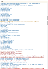
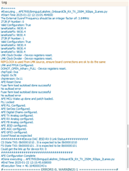
Please refer to the attached configuration script for additional details. after running the below script we are facing below errors in the Latte log.
#fpgaside 24410 afeside 12410 1 inst's are there ############## Read me ############## #In HSDC Pro DAC tab, Select AFE79xx_2x2TX_44210; Data Rate = 245.76M #In HSDC Pro ADC tab, Select AFE79xx_2x2RX_44210; Data Rate = 245.76M ---> To capture 4 RX channels sysParams=AFE.systemParams sysParams.__init__();sysParams.chipVersion=chipVersion setupParams.skipFpga = 1 # setup FPGA (TSW14J56) using HSDC Pro ############## Top Level ############## sysParams.FRef = 491.52 sysParams.FadcRx = 2949.12 sysParams.FadcFb = 2949.12 sysParams.Fdac = 2949.12*4 sysParams.externalClockRx=False sysParams.externalClockTx=False ############## Digital Chain ############## ##### RX ##### sysParams.ddcFactorRx = [12,12,12,12] #DDC decimation factor for RX A, B, C and D sysParams.rxEnable = [True,True,False,False] sysParams.rxNco0 = [[9500,9500], #Band0, Band1 for RXA [9500,9500], #Band0, Band1 for RXB [9500,9500], #Band0, Band1 for RXC [9500,9500]] #Band0, Band1 for RXD ##### FB ##### sysParams.fbEnable = [False,False] sysParams.ddcFactorFb = [12,12] #DDC decimation factor for FB 1 and 2 sysParams.fbNco0 = [9500,9500] #Band0 for FB1 and FB2 ##### TX ##### sysParams.ducFactorTx = [48,48,48,48] #DUC interpolation factor for TX A, B, C and D sysParams.txEnable = [True,True,False,False] sysParams.txNco0 = [[9500,9500], #Band0, Band1 for TXA [9500,9500], #Band0, Band1 for TXB [9500,9500], #Band0, Band1 for TXC [9500,9500]] #Band0, Band1 for TXD ############## JESD ############## ##### ADC-JESD ##### sysParams.jesdSystemMode= [3,3] #SystemMode 0: 2R1F-FDD ; rx1-rx2-fb -fb #SystemMode 1: 1R1F-FDD ; rx -rx -fb -fb #SystemMode 2: 2R-FDD ; rx1-rx1-rx2-rx2 #SystemMode 3: 1R ; rx -rx -rx -rx #SystemMode 4: 1F ; fb -fb- fb -fb #SystemMode 5: 1R1F-TDD ; rx/fb-rx/fb-rx/fb-rx/fb sysParams.jesdTxProtocol= [0,0] # 0 - 8b/10b encoding; 2 - 64b/66b encoding sysParams.LMFSHdRx = ["24410","24410","24410","24410"] #changed by Lakshmi ["44210","44210","44210","44210"] # The 2nd and 4th are valid only for jesdSystemMode values in (0,2). # For other modes, select 4 converter modes for 1st and 3rd. sysParams.LMFSHdFb = ["14810","14810"] sysParams.rxJesdTxScr = [True,True,True,True] #changed by Lakshmi sysParams.fbJesdTxScr = [True,True] sysParams.rxJesdTxK = [16,16,16,16] sysParams.fbJesdTxK = [16,16] sysParams.jesdTxLaneMux = [0,1,2,3,4,5,6,7] # Enter which lanes you want in each location. # For example, if you want to exchange the first two lines of each 2T, # this should be [[1,0,2,3],[5,4,6,7]] ##### DAC-JESD ##### sysParams.jesdRxProtocol= [0,0] sysParams.LMFSHdTx = ["24410","24410","24410","24410"] sysParams.jesdRxLaneMux = [0,1,2,3,4,5,6,7] # Enter which lanes you want in each location. sysParams.serdesRxLanePolarity = [1,1,0,0,0,0,0,0] # For example, if you want to exchange the first two lines of each 2R # this should be [[1,0,2,3],[5,4,6,7]] sysParams.jesdRxRbd = [4, 4] sysParams.jesdRxScr = [True,True,True,True] sysParams.jesdRxK = [16,16,16,16] ##### JESD Common ##### sysParams.jesdABLvdsSync= False sysParams.jesdCDLvdsSync= False sysParams.syncLoopBack = True #JESD Sync signal is connected to FPGA ############## GPIO ############## sysParams.gpioMapping = { 'H8': 'ADC_SYNC0', 'H7': 'DAC_SYNC0', #'ADC_SYNC1', 'N8': 'ADC_SYNC2', 'N7': 'ADC_SYNC3', 'H9': 'ADC_SYNC1', #'DAC_SYNC0', 'G9': 'DAC_SYNC1', 'N9': 'DAC_SYNC2', 'P9': 'DAC_SYNC3', 'P14': 'GLOBAL_PDN', 'K14': 'FBABTDD', 'R6': 'FBCDTDD', 'H15': ['TXATDD','TXBTDD'], 'V5': ['TXCTDD','TXDTDD'], 'E7': ['RXATDD','RXBTDD'], 'R15': ['RXCTDD','RXDTDD']} ############## LMK Params ############## lmkParams.pllEn = True lmkParams.inputClk = 983.04 # Valid only when lmkParams.pllEn = False lmkParams.lmkFrefClk = True setupParams.fpgaRefClk = 245.76 # Should be equal to LaneRate/40 for TSW14J56 ############## Logging ############## logDumpInst.setFileName(ASTERIX_DIR+DEVICES_DIR+r"\Afe79xxPg1.txt") logDumpInst.logFormat=0x0 #Modify to 0x1 to save register scequence to log file. Script takes more time to execute. logDumpInst.rewriteFile=1 logDumpInst.rewriteFileFormat4=1 device.optimizeWrites=0 device.rawWriteLogEn=1 device.delay_time = 0 #--------------------------------------# #setupParams.skipLmk = False #AFE.initializeConfig() #lmkParams.sysrefFreq = AFE.systemStatus.sysrefFreq #lmkParams.lmkPulseSysrefMode = False #AFE.LMK.lmkConfig() #-------------------------------------------------------------------------------------------------# AFE.deviceBringup() AFE.TOP.overrideTdd(15,3,15) # bit-wise; 4R,2F,4T #setupParams.skipLmk = 1 #AFE.deviceBringup() #AFE.TOP.overrideTdd(15,0,15) #setupParams.skipLmk = 0
In the design, we are configuring some of the internal registers of the JESD204C on both the RX core and TX core sides using the AXI protocol. We are sending counter data to the ADC while simultaneously collecting data from the DAC.
Upon receiving the GT_POWERGOOD signal, we assert the reset and, after a brief period, de-assert the reset. This reset process occurs simultaneously with the configuration of the AFE board.
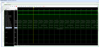
Currently, eventhough we got errors in log file,we are observing that the TX_RESET_DONE and RX_RESET_DONE signals are being asserted as expected; however, the SYNC signal is not coming from the DAC_JESD_rx or the RX_FPGA JESD. Interestingly, if I manually assert the reset again after configuring the AFE, the TX_SYNC signal is generated, but the RX_SYNC signal is still absent.
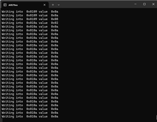
For further reference, please find the attached screenshot detailing the issue. If the RX_SYNC signal is not being generated, the ADC JESD_TX should be sending comma characters. However, I am observing random data instead.
In a separate scenario, I reset the system and started configuring the AFE board, but I de-asserted the reset before the AFE configuration was completed.This time is didn't get any errors in latte log,And I was able to observe both RX_SYNC and TX_SYNC signals; however, random data is being received from the ADC on the RX side, which does not appear to be correct. I have attached a screenshot for reference.
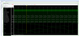
Could you please help identify where I may have gone wrong and confirm if the reset procedure I am using is correct? And Could you please help identify the cause of this behavior or confirm if there might be an issue with my configuration? Additionally, I attempted to send constant data using the Latte GUI, but this did not work either. Could you kindly explain how to proceed further?"
Hi Ajay,
I believe that the issue you are facing is caused by the bringup sequence. If the FPGA is not sending data to the AFE before device configuration then you would receive the errors you show above.
Can you try following the sequence below and see if that fixes the errors you are seeing?
Regards,
David Chaparro