This thread has been locked.

If you have a related question, please click the "Ask a related question" button in the top right corner. The newly created question will be automatically linked to this question.

CD74HC4051-Q1: Initial state of S0 S1 and S2 of CD74HC4051-Q1

Part Number: CD74HC4051-Q1

Hi team,

I have an application question which need your help.

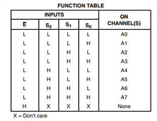
After the chip is powered on, what is the state of S0 S1 and S2? Does X mean high impedance? And if not, what would it be?

If the GPIO pin of C2000, which connected to S0 is set to input mode during use, what will be the impact?

Looking forward to your reply~

  • "X" means that it is allowed to be either high or low.

    S0/S1/S2 are high-impedance CMOS inputs and must never float. See [FAQ] How does a slow or floating input affect a CMOS device?

  • Hi Hangjie,

    When the /E is set to high, all the channels will be high impedance and there will not be an active channel no matter what the state of the S0, S1, or S2 pins are (X is a "don't care" in this case).

    In terms of the state of each on power on, that will be hard for me to say. If you ramp your /E pin with VCC, then they will be in a disabled state. Otherwise, if the /E is low, the voltage on the logic pins may be unknown and it could be registering as a high or low depending on the conditions of the circuit. In these kinds of situations, it is good to have a pull-up or pull-down to ensure the state of the logic pins at all times.

    Thanks!

    Bryan