This thread has been locked.

If you have a related question, please click the "Ask a related question" button in the top right corner. The newly created question will be automatically linked to this question.

CD4051BM96 signal distortion

Other Parts Discussed in Thread: CD4051B, SN74LV4051A

For some reason it doesn't recognize this part number. 

I recently edited a design we have been manufacturing for over a decade due to some product shortages. I had to change the voltage rail from +5v to +3.3Vdc. The device is being used as a multiplexar of analog signals into the microcontroller ADC. One of the legs has a severe decay of the signal after switching as well as some non linear behavior.

The analog signals are fairly static (mostly power supply monitoring) with voltages ranging from 360mV to 1.75 volts. The datasheet says that it should operate in these conditions without error. I am exploring the option that these might be fake parts and failure analysis from TI but have yet to find the smoking gun. Any thoughts?

  • CD4000 devices are designed for high voltages. At 5 V, the electrical characteristics of the CD4051B are much worse (see figure 3), and there are no guaranteed electrical characteristics for 3.3 V. I'd guess that the on-resistance is too high for your circuit.

    Use a low-voltage mux like the SN74LV4051A‍DR. (It is pin compatible if VEE = VSS.)

  • An alternate part is in the considerations. This does not address the fact that the data sheet says that it should and it has been reinforced on these forums. CD4051BM96 power supply voltage specification?

  • The datasheet says that the switch operates at 3.3 V, but it does not guarantee any upper limit on ron.

    What is the maximum source impedance supported by your ADC?

  • We've measure our Ron its only 470 ohm. Our voltage dividers provide a thevenin equivalant from 1.4k to 9.7k. I have not found any max source impedance requirements in the datasheet. Just some parameteters in the ADC registers for dealing with large impedance sources. 

  • Hey Joshua,

    There will always be some 'error' from the parasitics. You should expect some drop and as Clemens mentioned the CD405xB will perform worse at lower supply voltages. What are you actually seeing though? Can you describe or show some waveforms to further explain what sever decaying looks like? I suspect there will be a larger voltage drop but knowing what the actual drop is could also let us determine if it's within reason or not.

    Thanks,
    Rami

  • I realize their is a margin of error but right now I am 3 orders of magnitude of what I would expect. Please see the picture. And it is only doing it through one of our channels(see the one in the middle) (ignore the last one that is a known characteristic of one of the signals that is OK)decay

  • Hey Joshua,

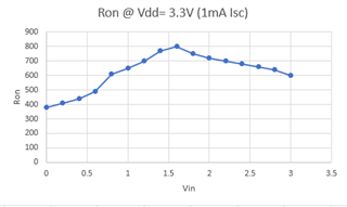
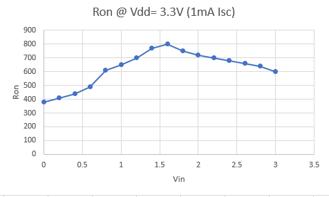
    I believe that you may just be seeing the RON having a greater affect on the curve when running at 3.3V. It looks like your input voltage from the waveforms is around 2.25-1.5V. Unfortunately, these conditions do show a pretty high RON peak which I suspect is affecting your settling time. I got a hold of some devices and ran an RON sweep at 3.3V with the following results : 


    RON looks to get up to 800ohms here, which could certainly be a source to that curve. I also saw that at 5V I didn't really see settling RC decay like I did at 3.3V so it makes sense that you didn't see it in your previous design.

    Unfortunately, some of these old datasheets aren't as concise as our more current ones (this one is from the 90's) so it doesn't look like we included a 3.3V curve to highlight this so I understand frustration with that. That being said, I know it may not be idle but if that settling time isn't desired, you may need to use the SN74LV4051A as a drop-in solution that is more geared for those lower voltages. 

    Thanks,
    Rami

  • This may be iof interest. We removed a chip from a failed board and placed it on a breadboard with no external load on the ouput. We then scaled the input voltage from 0-3.3VDC and you can clearly see that around 1-2VDC the output distorts significantly. Click here to play this video

  • I'm not able to actually see the image you sent. It may be a video though as i'm getting a plugin not supported error. Could you try resending or taking a snap shot of it?
    I'm sure though that 1-2V DC it would increase as that's where we really start to peak in RON according to the curve.

    Thanks,
    Rami

  • It is a video,Click here to play this video

  • as there was no load other than the oscilloscope probe reading it; i seriosly doubt a few hundred ohms would effect the 1meg resistance of the probe. 

  • Hey Joshua,

    So I've went into lab to take a better look at this, but also ran some simulations and do some calculations here to see if I can shed some light on this. Here are my results :

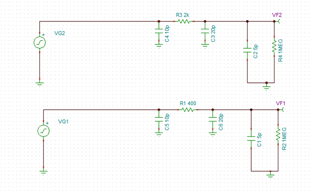
    So first off in some calculations, we can estimate this with the RC constant. The RC is just going to be the parallel combination of the RON and the probe and the parallel combination of the CON and Cload. I estimated the Cload of the probe to be 5pF here. The CON I simplified to being all 30pF on the drain side, even though this isn't entirely accurate (I'll show this better in the TINA simulation next). Note also that the RLoad and RON will see each other in parallel at AC so we'd want the parallel combination of the RON and Rload. 
    So using the thevenized circuit and RC the equation should be : RC = (RON*RLoad/RON+RLoad)*(CON + CLoad). 2 RC's will give us 86.5% of the charge/discharge. We'll take 86.5% to be close to the 10-90 rise time here. So to find the differences we can just do the follwing :

    2x(RON800*RLoad/RON+RLoad)*(CON + Cload)  -  2x(RON400*RLoad/RON+RLoad)*(CON+CLoad) where Rload = 1Meg, CLoad = 5pF, CON = 30pF, RON800 = 800ohms and RON400 = 400ohms. 
    I get about 28ns here. Well below what you saw. So I moved forward with simulation, since my approximations and assumptions or my math could just be off so to confirm I moved to TINA.

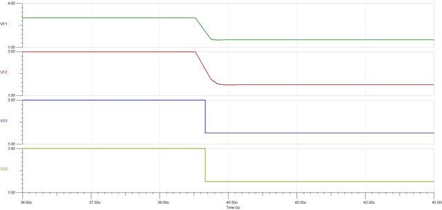
    I ran a TINA simulation of the equivalent circuit below. I added the CON and estimated a little bit on the CON of the source side being less than the CON on the drain side while keeping the values equaling the full 30pF. The probe is he load here at 1Meg and I estimated it would be roughly a 5pF load as well.

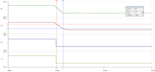
    You'll see in the results that the 10-90 does increase close to 2x. 

    I see a difference of close to 47ns in the model. So close to my approximations but still nowhere near what you're seeing. 

    So next, maybe we've mis-spec'ed this or there is something wrong with the performance in general of the device. So for this, I moved to the lab bench.

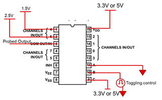
    I did the same setup here. I ran the device with a square wave on the control input and toggled between two channels going from 2.5V to 1.5V and changed the VCC from 5V to 3.3V. 
    I definitely did see some change in the settling time but nowhere near what you saw. I had to zoom in quite a bit to see a difference.

    E2E doesn't seem to cooperate with my images i'm trying to attach but i'll keep trying but I'm seeing closer to a 600ns transition time on the 3V3 case.
     Which makes sense as the models and the math don't include the transition time. The address to signal out transition time is spec'ed at 450ns typical at 5V. So given that I would expect it worsen a bit at 3V3 supply.

    I'm not certain if there is something in my setup that is different than yours so maybe confirm for me that I've done everything correctly but for now, I simply can't duplicate the issue you're seeing to this extent. What is the voltage source that you use here? I don't believe it would cause this great of an impact but it is worth digging into as well.

    I believe though that there is external communication about a failure analysis that maybe we can discuss further offline (I can send you an email or e2e message about this) but right now, I can't seem to duplicate this so until I can, I'm a little limited on the support from a technical support perspective.

    Thanks,
    Rami


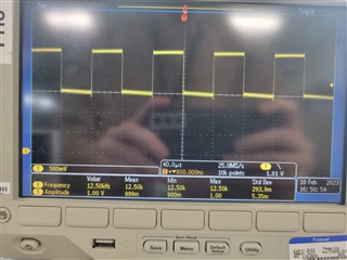
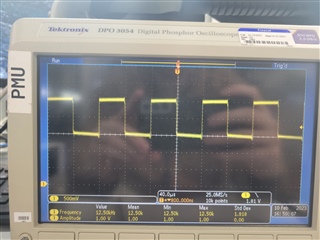
  • This is the 5V zoomed out view. I don't see any decay issues, which I believe you report as well


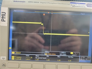
    When I zoom in I see just a couple 100ns for the transition.


    At 3.3V supply, I run the same test and it's hardly noticeable that anything has changed.

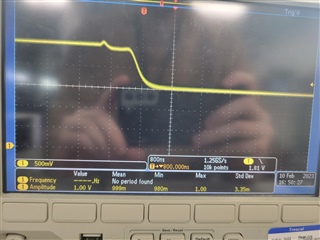
    There definitely is some change though, but only noticeable when I zoom in to a 800ns/div scale. There is a little artifact before the transition but I don't think that to be relevant to this. You'll see below though that the transition time here take a little longer. We'll see about 600-800ns. So about 4-600ns added on from changing the supplies from 5V-3.3V


    Here's the setup I used. Please let me know if anything is off here


    Thanks!
    Rami

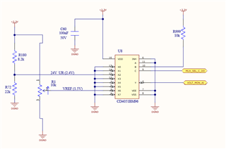
  • Thank you for the effort you have been putting into this. Your test is a little different than the the one we are running. Here is a picture.

    We are toggling betweend channel 2 and 6 using a signal generator at 10hz. R1 is then slowly adjusted so that Vref is scaled from 0-3.3V. This is what gives us the output I demonstrated in the video. When Vref hits that 1-2V range is where we see the demo in the video. 

    Thanks,

  • Hey Joshua,

    Thanks for this schematic, I'll try duplicating this exact same setup and see if we can find out what's happening here. I'll rerun tests tomorrow toggling between 2 and 6. In theory they should look the same across all channels and I had run some previous tests to check all channels and the results looked the same but I hadn't captured a screenshot, so I'll go back to the lab and double check for you and use the same setup with the same voltage divider on S2 and potentiometer on S6. I'll update you tomorrow.

    Thanks,
    Rami

  • Hi Rami,

    I have the same customer, probably from the same project and would be interested on the outcome if you were able to replicate this issue.

    Cordially,

    Art

  • Hey Art, Joshua,

    I've actually been able to replicate the behavior in lab. I've been investing across multiple devices and across multiple variables to determine what the root cause could be. Will update you on my findings. 

    Thanks,
    Rami

  • Hi Rami,

    Thanks for the update. According to our customer they sent parts for you guys to check. Were you able to replicate the issue on the parts they sent?

    Cordially,

    Art

  • Hi Rami, Team,

    Customer is looking for the availability of the Ron curve for 3.3 V operation, is that available?

    Best regards,

    Art

  • Hey Art,

    Yes, here is the curve. Note that this was a single unit on the lab bench.

    Thanks,
    Rami

  • Thanks Rami!

    Cordially,

    Art

  • Hi Rami,

    Just like to clarify, was the CD4051BM device the one used to generate the curve? If not, do we have the curve for the CD4051BM @ 3.3V?

    Cordially,

    Art

  • Hey Art,

    Yes this was done on a CD4051BM that was soldered onto a breakout board here in lab.

    Thanks,
    Rami

  • Hi Rami,

    Apologies for the late reply. I just received feedback from the customer and they are curious if we were able to determine the root cause and why they are seeing what they're seeing?

    They are curious since we mentioned that the device is nearly 25 years old and there hadn't been any recent returns or complaints like this one, hence wanted to know what could they be doing wrong.

    Thanks in advance.

    Art 

  • Art,

    I will reach out via email

    Thanks,
    Rami