This thread has been locked.

If you have a related question, please click the "Ask a related question" button in the top right corner. The newly created question will be automatically linked to this question.

WEBENCH® Tools/TPS40090: Unable to obtain result for Webench simulation

Part Number: TPS40090

Tool/software: WEBENCH® Design Tools

Hi,

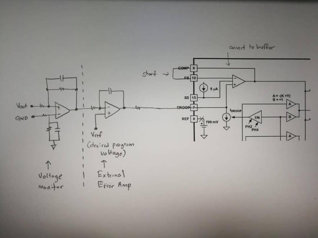
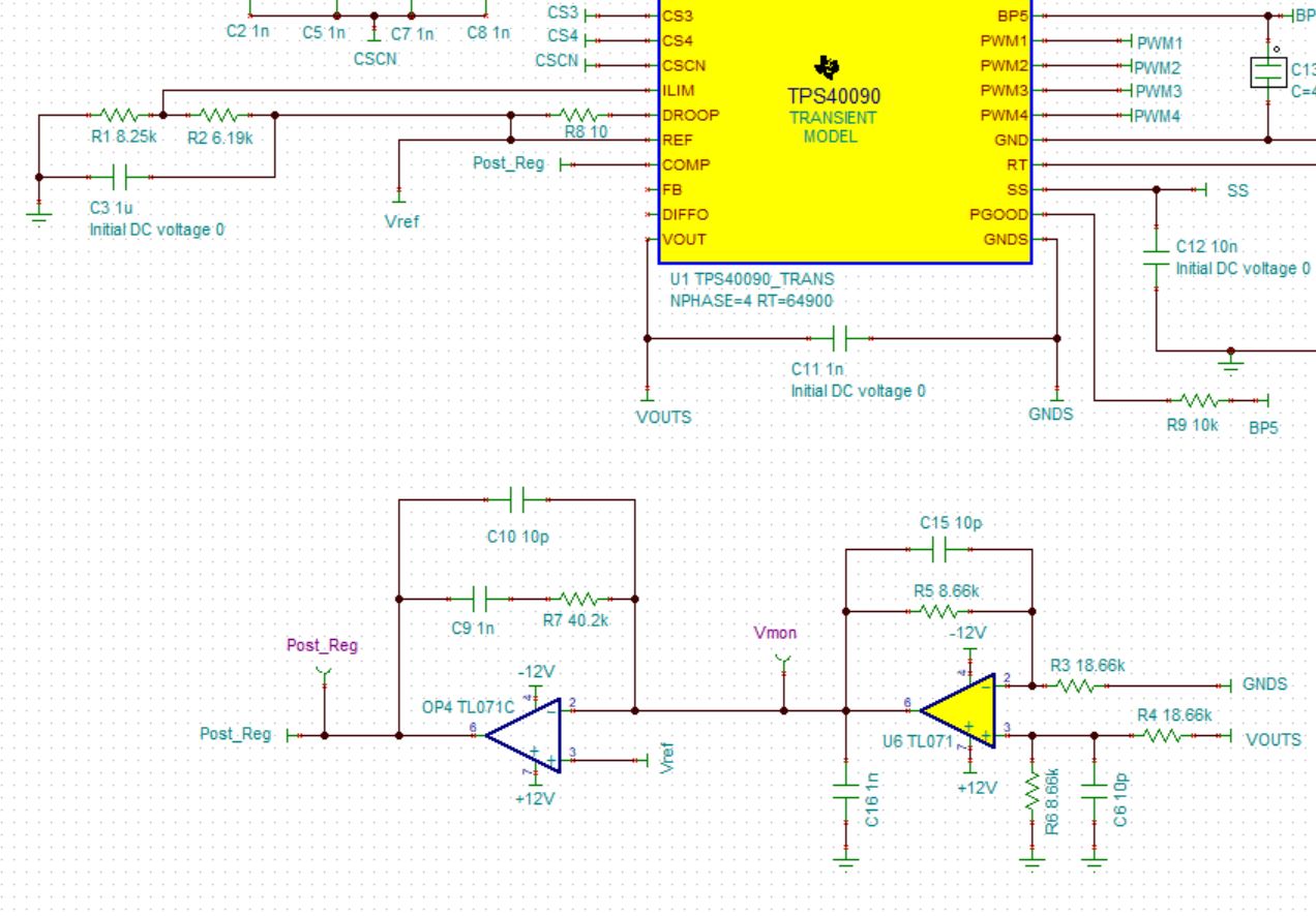
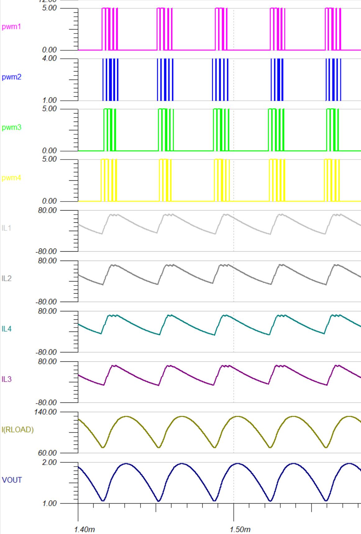
I'm facing difficulties in simulating the results for TPS40090 but unable to get the result. Would appreciate it you can look into the following.

I've tried connect the output of external error amp to bypass internal error amp but it's still not working. 

Regards,
Leo

  • Hi Leo,

    Sorry I did not reply by email due to urgent project I'm working on. 

    Can you apply a voltage source to COMP pin, to see if the simulation works?

    If it works, then problem should be related to external compensation circuit. 

    Thanks

    Qian

  • Hi Qian,

    If the COM pin is directly connected to voltage source, this controller will work on open loop condition and totally bypassing the error amp correct?

    Additionally, may I know whether the SS pin#15 is connected to the same feedback error amp? appreciate it if i can get a schematic/ref design on this section.

    Based on my understanding, the circuit will not work if I try shorting COM pin and FB pin to turn the internal opamp into buffer (change to external compensation circuit), this is due to the Idroop influence which cause the circuit unable to become pure buffer. Am I right?

  • Hi Leo, 

    1. The controller should work on open loop condition with COMP pin connected to voltage source directly. 

    2. I think SS pin does not mattter, because COMP is controlled by external voltage source. In simulation you can place a cap between SS and GND. 

    3. If COMP is driven by external voltage source, it is fine to short COMP pin and FB. 

    The reason I suggested to use voltage source to drive COMP is for debugging purpose. 

    We need to figure out if the issue from controller or from external circuit. 

    Thanks

    Qian

  • Hi Qian,

    I'm the person who is having this issues.

    I'm designing a buck converter using TPS40090 as the controller. This buck converter need to be a programmable one which means that i can control the output voltage based on the program voltage. This IC has a internal 0.7 voltage reference which can be disconnected. This is where i can connect my program voltage value.

    TPS40090 has internal error amplifier. My objective is to convert this internal error amp as a buffer (to bypass the internal error amp) and using external error amp with compensation.

    The reason why i want to use external error amp is because i have 3 control mode which is constant voltage, constant current and constant power which has its own compensation value. so i need to have 3 external error amp instead of one and feed it back to the internal buffer (which is the internal error amp converted to buffer) .

    I have tried doing this but the whole simulation is not working. I believe there is influence from SS pin and Idroop pin which in the diagram are also connected to the internal error amp, therefore the internal amp cannot be converted into pure buffer.

    Appreciate if you guys able to give some ideas regarding this issues.

  • Hi  Muhammad, 

    I replied in another post you submitted. 

    Thanks

    Qian

  • Hi Qian,

    I guess we should make this as the only thread from now on. Thank you for your feedback

    In your circuit, the loop will make COMP/FB voltage be equal to DROOP pin, it is not able to regulate Vout to external Vref. 

    I think the output of external error amp should be connected to COMP pin directly. 

    I have made the changes like what you have suggested. The pwm signal turn into discontinuous mode and the output voltage fluctuating. 

    What i did is i connect the output of the external error amp directly to the COMP pin while maintaining the original connection to DROOP, SS and REF pin.

    I wonder is there any influence from DROOP and SS pin to the internal error amp causing the circuit to behave like this. Can i get a more detail schematic of the internal error amp to have better understanding on the

    expected behaviour?. Below is the waveform and the circuit


  • Hi MUHAMMAD, 

    The droop voltage is the reference voltage of internal error amplifier. Since the internal error amplifier is bypassed, the droop voltage should not be related to the issue. 

    I guess the loop is not stable. For debugging purpose. can you just apply a voltage source on COMP pin and check if Vout is stable?

    If Vout is stable, the issue should be related to external circuit.