This thread has been locked.

If you have a related question, please click the "Ask a related question" button in the top right corner. The newly created question will be automatically linked to this question.

INA200: Transient on Vin+ and Vin- indicates overcurrent on the CPM output

Part Number: INA200
Other Parts Discussed in Thread: TIDA-00302,

We have a design with 3 INA200-circuits monitoring 3 separate outputs. The system power is 14V.
Due to the load characteristics, transients of about 28V (limited by transient protectors) are created when the load is switched off. This leads occasionly to that one of the INA circuits indicates overcurrent on the CMP output. This condition occurrs about 4 times out of 10, and affects the circuits randomly, even the ones with no load attached.

Vss feeding the circuits is a stabilized 8V and looks clean.

We have tried to lower the limit of the transient protection down to 15V, and this leads to a significant improvement. In this case, only the circuit that is connected to the load is affected.

Our guess is that a rapid increase in the Vin+ and Vin- relative to Vss is the cause of the problem.

We also noted, that if the feeding power voltage (Vss) is increased, leading to a smaller difference between the feeding voltage and the peak transient voltage, the problems diminished in the same way as if the transient protection voltage limit was lowered.

  • Hi user4644630,

    Thanks for using TI E2E forums. Can you please share an schematic of your circuits so I have a better picture of your setup?

    Regards
  • Hi Mayrim,
    have you find out something?

    Best regards
    Per-Åke
  • Per-Åke,

    Mayrim and I looked over your schematics and and discussed this a bit. If I'm not mistaken, you've got a 3-phase H-bridge driver circuit and you're monitoring each phase with a high-side shunt. Is that correct? I'll assume it is and move on. I see lots of diodes, some of which I assume are to handle flyback of the motor when the load is turned off. I don't see any input filtering on the inputs of the INA200, like we show in page 14 of the data sheet. This can help with transient suppression and noise. Another resource to review about transient spike suppression is the TI Reference Design, TIDA-00302.

    Lowering the diodes makes sense as to why the spikes are reduced. I can't say I have a reason off the top of my head for why raising the power supply would help. We'll review more tomorrow. If you have any, please fill us in on the results of any other debug you might have done in the mean time.
  • INA200 test.pdfHi Jason, thanks for replay.

    its one h-bridge and two on/off output and we monitoring each output with and high-side shunt.

    The current sens resistor is very low 0R0005 and the problem is the same without load connected!!.

    Attached is a drawing of a simple testconnection that induces the error and affects the circuits randomly.

    Its  enough to raise the supply voltage of approximately 16V to create problems. In this connection, it is "controlled" transients.

    We have tried to disconnect pin 2 ie no signal in at CMP this made no difference.

    It seems that a rapid change in voltage on Vin +/- incorrectly triggers CMP.

    In this case, the solution would be a filter that you describe in TIDA-0032.

    It is also on my drawing. The problem is that it also slows the useful signal, for example at

    short circuit of the output.

    This is a new product for us, and we have a first shipment of 1,000 units (being produced) and unfortunately we were not expecting this problem. Our customer and we discovered it unfortunately too late.

    So a smart solution is welcomed :-)

    The card handles 300 amp / output short circuit protected, delayed protection of normal current limit. Normally works INA 200 excellent.

    Best regards

    Per-Åke

  • Per-Åke,

    We tried a test setup similar to the one you provided, essentially jumping between 0V and 30V, no load, IN+ = IN-. We left OUT floating, and we monitored CMPOUT. We saw only 300mV (or less) ringing when the voltage was applied to IN+/IN-. We were never able to get the CMPOUT signal to transition. Perhaps we have it set up incorrectly?

    Can you provide an oscilloscope capture of IN+ and CMPOUT during these transient events, so we know what to look for?
  • Hi Jason,

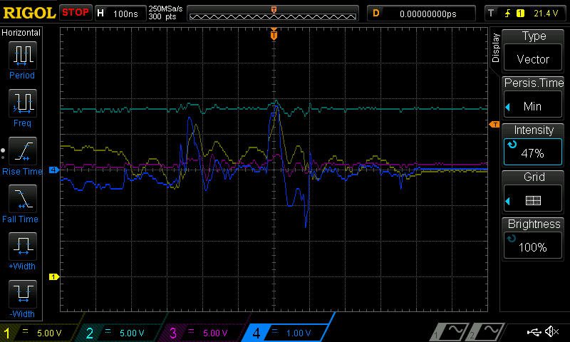
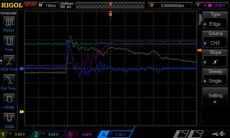
    attached you find oscilloscope capture, 1 input from powersupply and transient capacitor, 2 Vcc on pin 1 IC7, 3 CMPout IC7, 4 Out pin 2 IC7.

    Some noise because my "transient switch" is a bit too mechanical.
    Note that the output pin 2 follows  input supply

    The test setup is as earlier drawing.

    Best regards

    Per-Åke


  • Per-Åke,

    So these plots show that with a jump in common mode, the output of the device spikes up and then settles back down to its expected output state.  The OUT pin is not connected to the CMPIN pin in your test circuit, so it shouldn't have any way of triggering the comparator, correct?  Even still, with the common mode jump, the CMPOUT pin is triggered and goes to a high-state.  Is that all correct?

    I'm checking with our design team to see if they think there's a way for a common mode step to create a transient on the die that trips the comparator or something like that.  Also I'm going to debug the lab setup a bit more and see if I can better recreate this and then see what can be done to mitigate it.

  • Per-Åke,
    In your test circuit, is CMPIN tied to anything? The typical application has it tied to a resistor divider from OUT, but I was under the impression you didn't do that. I ask because in my setup, when I leave it floating, it floats somewhere above the 0.6V comparator trip point, so no matter what common mode step I put in, it is already tripped.
  • 2017-03-09 i sent drawings of the circuit board and this is the objekt under test.

    R 65 3k9 (for delayed low fuse)

    R 42 82K (for fast short Circuit protection)

    R43 10k

    Out in the field, we have tried to remove R56. Despite this, we still had problems with activity on CMP

    I attached a Picture of the card.

    Per-Åke

  • SORRY!

    Out in the field, we have tried to remove (WRONG!!!R56) R65 and R42. Despite this, we still had problems with activity on CMP.
  • hello Jason,
    have you find out something?

    Best regards

    Per-Åke
  • Per-Åke,
    We are revisiting this issue now and are going to try to recreate this behavior again. Assuming that we can, we will then try to mitigate it and let you know what we did to do so. Thank you for your patience.
  • Per-Åke,

    We are still unable to replicate your fault condition.  However, in recreating your test circuit, we have a few questions.

    What are the values of R1 and C2 in this circuit?

    When you say the OBJEKT has no load, does that mean the load is completely disconnected after the shunt resistor?  We are assuming that the shunt resistor is attached at J2.

    Have you tried removing the two filter/protection caps I highlighted below?

    Have you tried adding a differential cap as I drew in red?  This is a more typical filter network for a current shunt monitor.

    What are pins 2, 3, 5, 6 actually hooked to, or are they just floating?

    We have tried a few configurations and while we see some transient noise on the OUT pin from the large common mode step on the inputs, it is never over 300mV, and certainly after a resistor divider, the CMPIN would not see anything in excess of the 600mV necessary to make the CMPOUT change.

    In the plot below, Yellow is the common mode step on the bus voltage, and light blue is the OUT pin.

    We had a few other questions about the application that may shed some light on this -

    What is the nature of the load generating the dump on the bus?

    How fast is the short circuit protection requirement?

    Can the signal be filtered to remove transients before the comparator?

  • R1 100R

    C2 470uF low ESR

    The "OBJEKT"  is a complete circuit board according to previous drawings and photos and J4-J7 is not connected = NO LOAD!

    As I have shown in previous oscilloskopdump pin 2 follow incoming power (J2).

    As i told you earlier the shunt resistor is 0R0005 so i do not think a filter is an solution, we have the problem without load, so pin 7 and pin 8 is effectively shorted together.

    Please review the drawings that I sent, there are filter the signal before the comparator.

    /Per-Åke