This thread has been locked.

If you have a related question, please click the "Ask a related question" button in the top right corner. The newly created question will be automatically linked to this question.

INA240: Nyquist frequency sample rate

Guru 54118 points
Part Number: INA240
Other Parts Discussed in Thread: EK-TM4C1294XL, TIDA-01159, TIDA-01141

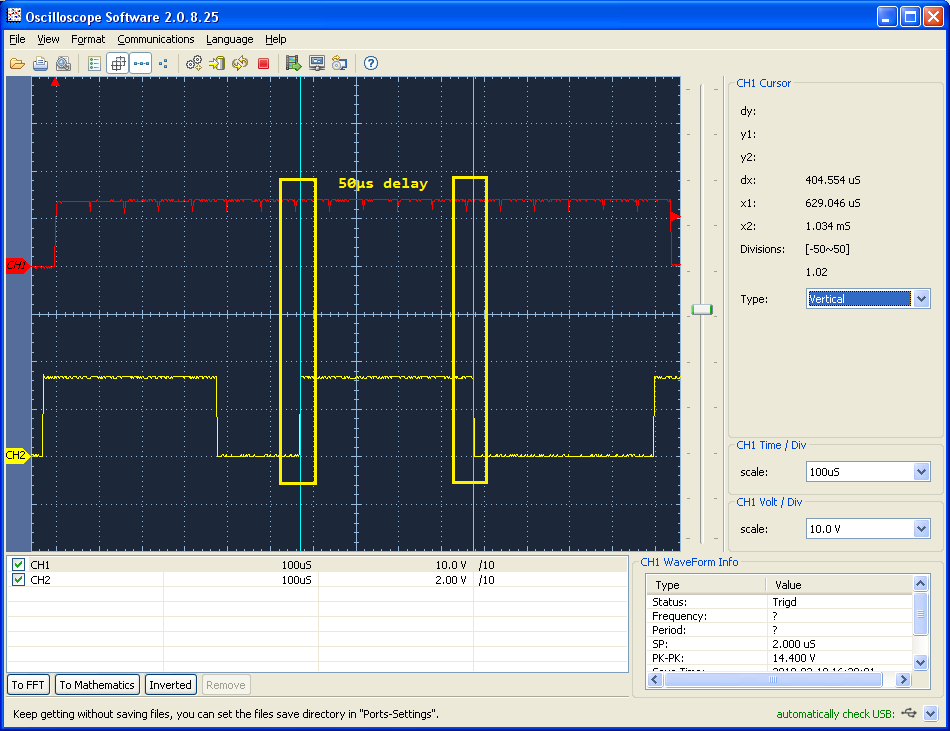
Why does A1 output require a substantially reduced sample blanking time, well below 2x Nyquist sample frequency? The fastest Nyquist rate sample frequency (4.1KHz) possible via 2mohm shunt, 20KHz PWM signal, low side monitor is 240us @2MSPS via TI 12 bit MCU embedded ADC. Any attempt to sample the A1 output signal at a faster Nyquist frequency or rate just above 9.6us A1 setting time produces very low sample values and very inaccurate voltage to current conversions. 

Attempting to trigger ADC mid PWM pulse width (25us) to sample A1 output simply produces very low and incorrect RMS current measures. I would expect some SNR error from the 12 bit ADC but not to the point it affects the Nyquist sample rate. Supposedly the 240 PWM rejection transient input filters (as is) reduces spurious out of band harmonic signals so PSRR/CMRR remain fairly consistent to datasheet graphs. Please help me to comprehend how simple low side monitor can not achieve excellent results via 12 bit ADC less than 2 inches away from even six 240 buffered signals on the very same PCB circuit. I don't suspect an issue with the 12 bit ADC or software timing since GPIO debug of scope captures remain/are consistent with/to PWM 25us sample points yet very low value RMS results. 

https://en.wikipedia.org/wiki/Nyquist_frequency

https://en.wikipedia.org/wiki/Nyquist_rate

  • Capture 2msps sampling 400µs Nyquist frequency with GPIO watch dog to confirm the software is indeed keeping synchronous to/with the A1 and ADC blanking trigger. Yet as one can see the very slow Nyquist frequency was/is required so ADC can achieve any kind of error free convergence. As mentioned the fastest banking time always requires 6 PWM periods to sample the (back half) of the inductive current wave form instead of each and every PWM period @25µs. The best I was able to reduce the Nyquist sample frequency by almost 1/2 to 240µs (not shown) to achieve fairly accurate ADC convergence.

    Perhaps the 240 narrow bandwidth (46KHz) causing issue but how to work around other than reducing the Nyquist frequency? The Nyquist sample rate of ADC (2MSPS) can not be reduced....

    Note the ADC is level triggered sample convergence @150ns. Capture shows 12.5KHz PWM low side shunt 240 output CH1

    Worst case settling was first believed to require 400µs blanking ADC trigger  CH2, best case 240µs (not shown). Infers the 240 output is not considered settled @9.6µs in order to achieve <1% precision across the SAR ADC sample spectrum (2MSPS).


  • Hi BP101,

    From your description I’m under the impression that INA240 output is not an accurate representation of what it should be. If this is the case, can you overlay the ideal output on the scope shots? A hand sketch should be good enough. This will help understand the problem better.

    Regards, Guang

  • Hi Guang,

    Guang Zhou said:
    From your description I’m under the impression that INA240 output is not an accurate representation of what it should be

    Do you see something in the captured (20KHz)  signal or any signal that would prohibit rapidly sampling at 2x Nyquist frequency, e.g. (25us/40Khz),  >Nyquist rate (2MSPS)?

    Surely TI has an answer for why their own 12bit SAR ADC refuses to properly charge share 240 open loop signal or converge near 1/2LSB or even 1/4 LSB?

    Oddly the only way to achieve the correct LINEAR magnitude in the Nyquist frequency requires >200us between samplings of 240 output. Why is that?

  • Hi BP101,

    There are two possibilities:

    (1)   INA240 output is correct, however the ADC measurement is not if it samples faster than 200uS per sample.

    (2)   INA240 output is incorrect and consequently ADC measurement is incorrect.

    Which one is it? Can you confirm? I’m guessing (1) otherwise you should have questioned the scopes shots themselves not the measurements.

    Regards, Guang

  • Hi Guang,

    Guang Zhou said:
    Which one is it? Can you confirm?

    Seemingly a deflecting answer as TI is seemingly unaware of analog saturation, results from 240 output structure/s.

    Seemingly +/-IN (shunt) SNR levels effect 240 output linearity thus directly impacts Nyquist frequency (40kHz) in the open loop charge recovery time of the SAR. Seemingly forensic analysis proves PWM rejection is causing some kind of mayhem in the Nyquist frequency!

    A Wiki report would go a long way to help the community identify such issues.

  • Hi BP101,

    First of all, I asked a strictly technical question in order to clearly define the problem – be it device related or system related. That is by no means an answer, let alone deflecting. I think it is straightforward and I'm surprised you refuse to answer.

    Until you can either concretely prove this is a INA240 issue, or work with us to identify this an INA240 issue, there is no more I can offer.

    Regards, Guang

  • Guang Zhou said:
    First of all, I asked a strictly technical question in order to clearly define the problem – be it device related or system related.

    You answered a post with a question requiring an answer to the posted question. The answer to your question/s is the threads question being asked - nothing more.

    I can't say either one, TI needs to investigate how the lack of Nyquist frequency response might be systemic to either of their devices. What might lead to or be the cause of linearity break down in either one of the devices?

    I greatly suspect the Nyquist frequency is being distorted by PWM rejection, though it could even be bandwidth related. The only thing I can do on this end is install competition current monitors and determine if the Nyquist frequency is then normalized or the ADC samples then improve in linearity. The software is working as expected however other testing seems to indicate the signal quality may have some thing to do with ADC samples linearity being distorted. Baffling part is the captures appear mostly normal other than sporadic transients every few seconds. Yet peak transients are not supposed to exist according to datasheet so they must be RF based picked up by digital scope probe. Real time scope widgets do not have any scaled spikes as one might expect and past have occurred via FAN7174 discrete Opamp current monitors.  

  • Hi Guang,

    TI technical library suggest ADC blanking time for in line monitor (Fig.4) can be reduced via PWM rejection.  This statement directly in opposition to 240 low side monitoring blanking.  PWM rejection seems to require abnormally large blanking time >200us. The other part being the current wave form being discussed is sinusoidal, not trapezoidal. The entire document touts the INA240 reduced blanking based on in line current monitor with a very specific PWM class.

    This method does not stress test the INA240 for industry typical PWM, low side monitor use! Space vector PWM is/was not considered typical even by TI earlier motor RDK we purchased. Trapezoidal waveforms produce 240 output above post. Perhaps TI should allocate some engineering time to investigate why ADC blanking time must be increased >200us for low side monitoring. The goal being to arrive at correct 20Khz PWM Nyquist frequency (40KHZ) @2MSPS with conversion trigger blanking time <200us. 

    https://e2e.ti.com/blogs_/b/motordrivecontrol/archive/2016/11/08/five-benefits-of-enhanced-pwm-rejection-for-in-line-motor-control

  • Hi BP101,

    Here is a INA240 step response plot from the data sheet. The necessary time would be from the start of the step input to wherever the settling requires it to be. For example, sampling can start at 10uS, then the real (or necessary) blanking time would be 10uS. 

    When you say 200uS is required, can you please illustrate on a similar plot to show the start point of this time period?

    Regards, Guang

  • Guang Zhou said:
    can you please illustrate on a similar plot to show the start point of this time period?

    The posted scope capture is the real time plot of blanking >200us. Seemingly you do not fully grasp what is being described in thread text or would not be asking this question.

    CH1 = 240 output (OPAMP), CH2 = GPIO marker indicating ADC edge triggered window (blanking) required to achieve conversion of sampling events (150ns). The GPIO does not trigger the ADC rather a GPTM timer does, beginning of each PWM commutation. As you can clearly see the Nyquist frequency was 2x 12.5KHz(160us) in above capture. However the same issue occurs even at 20KHz or 2x Nyquist frequency 40Khz >200us is required to achieve proper samples in the Nyquist frequency no matter what 240 datasheet graph indicates. Again datasheet graphs indicate VS=+5v and not +3.3v.

    TM4C1294 MCU datasheet only states the ADC conversion is an edge triggered event, in this case 4 samples should occur over 6 PWM commutation events. Trying to sample this signal at the Nyquist frequency produces incorrect very low readings. It will require TI laboratory time to determine what if any aspect of PWM rejection may lead to low side monitoring issues at the Nyquist frequency that is science based not forum conjecture.

  • Hi BP101,

    You're right, obviously I don’t fully grasp what you described in thread text. Therefore, can you label on the plot what correspond to time (200uS blanking being one of them) and frequencies? It is not obvious to me what you’re talking about.

    Regards, Guang

  • Guang Zhou said:
    Therefore, can you label on the plot what correspond to time (200uS blanking being one of them)

    Capture is labeled: CH2 (GPTM4) represent the edge event/s of ADC sample trigger blanking interval/s in output signal CH1. The word blanking infers added delay time in this context. Since the ADC trigger is an edge event it therefore occurs 4 times in the posted capture of 6x 80us periods. In reality blanking needs to occur center of each of the 6x 80us periods CH1. As stated several times it is impossible to achieve accurate results sampling CH1 @ 2x the Nyquist frequency (160us), in the case of 12.5KHz PWM signal.  When the PWM is 20KHz (50us), 2x Nyquist frequency needs to occur @ 25us/40KHz, yet samples still results in much lower amplitudes being detected by ADC.

    Each saw point CH1 signal are ends of 12.5KHz(80us) 6 periods, any attempt to sample CH2 signal in the center of each 80us periods produces incorrect results. The difference being the industry standard Nyquist trigger time is much faster @25Khz(40us). The ability of 240 to maintain consistent linearity in the settling time becomes more critical. It seems the datasheet conclusion 9.6us setting (A1) is related to inline monitoring and strays under certain conditions.

    Thus settling CH1 though it seems visually ok above capture, must be slowed >200us(5KHz) to capture anywhere close to correct values. Only a very expensive Tektronix storage scope with time delay sweep can properly analyze the signal for perturbation issues in this settling question. Seemingly laboratory analysis 240 settling may not reveal how PWM rejection may or does alter value of settling when the PWM duty cycle is rapidly changing in low side monitoring positions. That seems the only logical conclusion in my mind, the brain teaser is the visual aspect of typical digital scope samples (1/10KSPS) deep can not reveal the 240 output settling is actually >200us relative to GPTM4 marker. 

    The question returns to why can PWM rejection interfere with the Nyquist sample frequency perhaps only while low side monitoring? As you can read in Wiki links the Nyquist sample rate is often much faster 2MSPS in our case.   


  • Hi BP101,

    It doesn’t help to simply state that your system works in one setting, not the other.

    You made it sound like a settling problem, ie, INA240 takes more than 200uS to settle, which apparently is not true.

    If you believe it is an INA240 issue, please be specific and concise in demonstrating it. So far, I cannot draw that conclusion based on information you provided.

    I suggest use diagrams and illustrations to make your point. Yes you did post a couple of scope shots, but how are they related to your argument?

    Regards, Guang

  • Guang Zhou said:
    Yes you did post a couple of scope shots, but how are they related to your argument?

    And that capture does not indicate something is terribly wrong to you? If not perhaps you do not have the experience necessary to determine why INA240 can not be sampled by TI embedded SAR ADC at 2x the Nyquist frequency.

    This is not a customer problem of circuit analysis, it is a TI problem to verify 240 is even producing precision results as intended in the scenario depicted as low side current monitor. The datasheet gives no conditions under which 9.6us setting occurs other than best case sine wave input. Why does TI refuse to test the 240 under inductive PWM current load >5 amps? Speculative laboratory testing easily refuted under PWM analysis would reveal a breakdown occurs. Perhaps the manufactured should be dam sure proper precision via 240 is even possible when placed into low side monitor positions! We have proven it does work yet suffers greatly to hold to the datasheet specification (9.6us settling) when real time motor PWM has been injected into +/-IN ports.   

    FYI: The SAR ADC only processes 240 signal "when ever AD converter considers the signal settled" typical conversion (150ns) yet the 240 open loop gain settles >1/2 LSB. Again the capture shows worst case settling occurs @420µs. Best case settling for any 240 precision requires 240us settling time for ADC to produce correct samples, that is more than 6x the Nyquist frequency.

  • Hi BP101,

    That’s exactly why I requested you to explain how you determined that INA240 output is not right from the scope plots. How did you know the waveform is not what INA240 is supposed to produce? Couldn't it be “garbage in garbage out”?

    You said “real time motor PWM has been injected into +/-IN ports.” – Can you explain how the PWM comes about and how it looks like? I’m very curious to learn about this.

    I only know how INA240 is supposed to work; nothing about your system. With this in mind, try to explain in a way that is easy to understand.

    Regards, Guang

  • Guang Zhou said:
    Can you explain how the PWM comes about and how it looks like? I’m

    It comes from 3 PWM generators overlapping duty cycles low side 240 monitors. How else did you think CH1 in scope capture occurred? 

    Like I said perhaps issue requires very expensive storage scope to detect when the 240 output is actually considered settled relative to any TI 12 bit ADC ability to converge on the signal <200µs. That is way the Nyquist frequency is 6x greater than it should require and undermines the false narrative of 6.9µs setting time is even true. Stating the output settles 9.6µs is a mute point if the quality of the signal has to much edge jitter for an ADC to converge upon in that  same time.

    Again PWM/Transient rejection is supposed to clean up the signal so the ADC should not require >200us settling between each sample to produce precision digital measures. Again best case scenario 240µs is required to obtain any kind of precision from the signal on CH1. No scope capture can depict real time edge jitter and is therefore a point that can not be shown but only perhaps via video mpg file. Our Tektronix 2430 150Mhz  storage scope has a bad channel and Tenma newer 30Mhz scope is 1-10KSP deep has no delay function to even capture this issue in play.  

    Guang Zhou said:
    I only know how INA240 is supposed to work

    I don't believe any TI example (TIDA) application has ever tested the INA240 (low side) PWM monitor can produce any kind of precision results in 9.6µs setting via TI 12 bit SAR ADC. Again asking TI engineers preform due diligence and check reported issue of why TM4C1294 MCU 12 bit ADC struggles to converge on a signal that is claimed to be settled in 9.6µs! There are plenty of EK-TM4C1294XL launch pads to connect TIDA. The 100 amp TIDA http://www.ti.com/tool/tida-01141?jktype=design# Only need 150-200vdc inverter, BLDC motor to test it against.


  • Hi BP101,

    Everyone knows PWM is involved in a 3-Ph motor driver. What is new to me is how a low side current sense amplifier experiences this PWM. Perhaps you can shed some light on this since you repeated mentioned PWM interference. Once we understand what this PWM on INA240 input looks like, then we can talk about its interference and how to mitigate. Do you agree?

    Regards, Guang

  • It looks like the scope capture CH1, the stair steps are 6x 80us PWM periods in the 1.1ms entire wave. What you don't see are the random some times very high peaks at the tips of the steps.

    Below captured long ago was impossible for ADC to sample with blanking timer configured >25µs or a PWM event trigger 2x Nyquist frequency (40µs), exact center of each period a sample is take. The 240 was configured as bidirectional low side monitor +1.224v precision REF1,2 and a low pass filter on 240 output comprised of two series resistors 1nF to 10nF and even high as 22nF to improve acquisition time. Added filter capacitance causes transient comparator fault issues. Judging from the scope capture all appears ok but was only 1KSPS deep on the Tenma. Even with this much extensive filtering there was obviously to much output jitter for the ADC to converge in 40µs intervals. Never attempted blanking >200µs back then because it was not so obvious. It was a later hypothesis that lead me to testing higher Nyquist frequencies, AKA 6x Nyquist being the >200µs blanking intervals.


  • Capture above represents two overlapping PWM signals and the ensuing 240 output. They are not complementary paired PWM used in TIDA-01141 with TIDA-01159 isolated gate driver inverter. Complementary PWM seemingly does not produce the same peak inductor currents for magnetic flux changes in magnets of BLDC rotors as does overlapping PWM.  

    Why does it matter.. The complementary PWM inverter produces a smooth sinusoidal wave form apposed to the sharp peaks noted in the above posted capture. Somehow center aligned overlapping PWM signals monitored via 240 input do not produce Linear 9.6µs setting times. The SAR ADC does not consider the output settled in order to maintain precision even to <100% error across the entire shunt current range even @25µs. The loss of 240 adhering (theory) Nyquist sample frequency relative to SAR ADC, common practice of low side monitoring. Therefore the 240 output settling time for Non-complementary PWM signals relative to 12 bit SAR ADC is >200µs, never even close to datasheets touted 9.6µs.. 

    The 240 device obviously requires extensive INPUT filtering in opposition to several datasheet claims PWM/Transient rejection resolves typical issues other INA class monitors had previously reported. The question remains how much filtering is required and will that effect precision beyond that which is even practical? Does added input filtering reduce 6x Nyquist sample trigger frequency <2x industry typical? All very important questions relates to PCB redesign should not be the customers pit fall!

  • Up to now I have been referring to some kind of setting issue effecting the Nyquist sample frequency. Perhaps propagation delay is to blame if the Input slew rate falls behind the outputs ability to produce synchronous real time current events. I haven't attempted to check via scope since the datasheet gives no indication of propagation delay ever being effected by PWM rejection.

    Perhaps MAX40056FAUA+ may provide clues as to why 240 Nyquist sample frequency is 6x greater than expected.

    MAX40056FAUA+ is a bidirectional current-sense amplifier with an input common-mode range that extends from -0.1 V to +65 V with protection against negative inductive kickback voltages to -5 V. This current sense amplifier is well-suited for phase current monitoring of inductive loads, such as motors and solenoids, where pulse width modulation (PWM) is used to control the drive voltage and current. The MAX40056 uses an improved technique to help reject common-mode input PWM edges with slew rates up to and beyond ±500 V/µs. Common mode rejection ratio (CMRR) is typically 60 dB (50 V, ±500 V/µs input) and 140 dB DC, typical.

    https://datasheets.maximintegrated.com/en/ds/MAX40056F-MAX40056U.pdf

  • Hi BP101,

    If you keep the INA240 in linear mode of operation, there shouldn’t be noticeable delay, this is evident from both the data sheet step response and some of the scope plots I posted before to address your slew rate question.

    If you suspect otherwise, you need to capture the INA240 differential input voltage (or alternatively, load current) and the INA240 output in order to be able to tell. If you have such scope captures, please post it here.

    Regards, Guang

  • Hi Guang,

    Guang Zhou said:
    this is evident from both the data sheet step response and some of the scope plots I posted before to address your slew rate question

    However the step response does not indicate PWM rejection slew rate testing for sharp input edges. Only logical to compare the competition device may reveal the weakness I have been describing.

    What is the maximum PWM rejection slew rate/voltage of the A1 +/-IN, Is it 500v/µs? The TM4C1294 ADC converges in 150ns so this may explain how PWM rejection is phase shifting >200us sharp peaked pulses into the pass band of the amplifier. That slew phase shift might explain the random sharp peaks that roll through the pulse trained signal with no explanation to what they even originate from.  

  • Guang Zhou said:
    If you suspect otherwise, you need to capture the INA240 differential input voltage (or alternatively, load current)

    Indeed already present 1st capture posted, CH2 indicates delayed 150µs relative to CH1 signal trigger source. CH2 is GPIO port that represents the GPTM loaded with >400µs blanking, later reduced to 240µs.

    So why is the 240 output delayed by 150µs unless PWM rejection has delayed the +/-IN signals on the Out pin. Also any 240 internal breakdown, customer can only witness results from the outside. Does 240 work under stress perhaps it does, is it effective as low side current monitor (definitely not).

    The remaining 50µs is noticed capture (below) CH1 represents 18x 80µs PWM periods, each of 18x low (SW determined) are 150ns sampled results interrupt subroutine occurs synchronous to low side PWM gate drive. So the 150µs + 50µs = 200µs &  SW trims blanking timer +40µs to fine tune for delay periods. The 240 output delay (GPIO markers CH2) occur no matter what value blanking timer has been loaded to compensate, this capture markers are >400µs. Again the shortest total SW delay to compensate for 240 output delay is roughly 240µs, (not shown). No matter 9.6µs settling time of 240 output.

  • Hi BP101,

    You’re right that we can only witness the INA240 from outside. That’s why we need to know at least its input and output prior to making the judgement whether delay is excessive. There are several steps between activating a control signal to INA240 responds to change in current. A number of things can go wrong in between. It is impossible to blame it on INA240 without knowing what is fed to it and what it spits out. BTW to To provide this information, it does not require you to know anything of INA240’s inside.

    Regards, Guang

  • Hi Guang,

    It would seem that TI engineers would rather banter about a reported problem rather than investigate why the 240 is failing in the described way. It matters not what the customer presents as a signal in/out rather that the 240 is failing but why? It seems evident the competition is aware the necessary counter measures required for PWM rejection to properly work under high inductive kick back were omitted on the 240. Perhaps it is time to Tweak the 240 design correcting issues for the past reported seemingly obvious phase shifted inversion? 

    Will TI investigate why A1 or A2 appears to phase shift +/-IN signal output causing delay of ADC sample results >200µs. Scope CH1 is inverted so the CH2 signatures can be properly witnessed in time domain.

  • Hi BP101,

    TI takes customer issues very seriously. If such an issue is found to be indeed caused by our products, corrective actions are  taken.

    The debug process is team work however. It requires customer’s help to isolate the issue into manageable parts. It is one of such isolation process to show what the input/output is to our device.

    Regards, Guang

  • Guang Zhou said:
    It requires customer’s help to isolate the issue into manageable parts.

    Yet posted capture was presented to this forum about shunt inversion question. It seems obvious >400µs shift occurs on output of the inverted signal relative to +/-IN. It would seem what ever test TI used to determine transient response rise/fall time + settling did not consider these >400µs phase shifts occur in PWM rejection. Transient analysis graph perhaps did not reveal phase shifting (CH2) occurs due to sharp PWM peaks (CH1).  

    If sharp PWM peaks (CH1) were effecting other ADC samples seemingly the three channels detecting edges for the commutation timer would require very same 240µs sample delay. Fact is all other ADC channel processing is functioning correctly, seems to point the finger at 240 somehow delaying the 3 monitored signals. 

  • Hi BP101,

    Please confirm:

    (1)    CH1 is measured at positive input pin (IN+) of INA240, relative to ground.

    (2)    CH1 is inverted as indicated on plot by red text.

    How can you tell there is a “>400µs phase shifts” from the plot? Can you be more specific on this?

    You’ve been talking about a ~200uS delay. Is there a relationship between the two, or are they separate issues?

    Regards, Guang

  • Correct to both questions, CH2 has a 2RC low pass filter into ADC channel. Visual inspection clearly reveals a phase shift has occurred and accounts for 200-400µs delay being required to compensate for large very random (PWM duty cycle) propagation delay of output signal. Again 400µs is 6x the Nyquist sample frequency and 3x Nyquist (~200µs) can capture the envelope, center of periods with a bit more precision. Otherwise if the delay is omitted the monitored results are highly flawed. 

    Perhaps TI can verify why Sharp PWM pulses of other unknown artifacts effect PWM rejection in this way.

  • Hi BP101,

    Please label/show on that scope plot, how you can tell there is a “>400µs phase shifts”.

    The other comment I have is that PWM interference shouldn’t be an issue for a low side sensing like yours. This shouldn’t have been part of the discussion. Unless there is coupling.

    Regards, Guang

  • Guang Zhou said:
    Please label/show on that scope plot, how you can tell there is a “>400µs phase shifts”.

    Ok it is the original capture. I simply never considered propagation delay of A1 causing this issue. FB electronics forum posted same capture, several engineers see the shift too. One can't easily see the delay until scope has one channel inverted and overlays both signals. Even though each pulse settles 9.6µs, the input  signal is phase shifted and inverted on the output. That is how the inverted shunt CMV is right side up on the output in my other captures.

    AKA no need to re-invert the output as the input was already inverted by 240 for sampling by the ADC channel. 

  • Hi BP101,

    If you can’t show there is a “>400µs phase shifts” at this moment, I suggest you collect the relevant evidence and come back when you’re ready.

    Regards, Guang

  • Hi BP101,

    I will close this thread for now. Please post back when you have new information that we discussed.

    Regards, Guang

  • Hi Guang,

    Guang Zhou said:
    If you can’t show there is a “>400µs phase shifts” at this moment

    I was away on business but had updated the thread capture as you requested. Original thread posted capture seems to indicate >400us phase shift or propagation delay via vertical markers.

    Posted below once more for your viewing enjoyment.

  • Hi Guang,

    I was away on business but had updated the thread capture thus indicating >400us phase shift or propagation delay via vertical markers.

  • Hi BP101,

    Why did you pick these two points as start/stop of the “400uS delay”?

    Regards, Guang

  • Guang Zhou said:
    Why did you pick these two points as start/stop of the “400uS delay”?

    The 2 vertical points represent the beginning of the PWM cycle (80us) periods in each channel. Has TI even yet attempted to investigate how -4v inductive kickback or slew rate <±500v/µs on +/-IN might lead to any In/Out propagation delay? The output or input channel (either one) must be inverted on the scope to witness the slew rate propagation delay. Again with or without an output filter the same delay occurs.

  • Hi BP101,

    INA240 output waveform is tracking the input voltage waveform from that picture, both are saw-tooth. That 400uS is not a delay from the INA240’s perspective.

    Regards, Guang

  • The signal input is PWM not saw tooth and CH2 is the trigger source. There was plenty of acquisition time in each PWM filtered pulse for the ADC, so we can't blame ADC for propagation delay.

    From the ADC perspective "the only one that counts" the phase shift (Input to Output) is enormous, relative to 240 signal acquisition. Oddly the 240 datasheet has not listed any propagation delay what so ever, under any conditions.

    Even the MAX40056F data sheet indicates 500ns propagation delay with counter measures to reject inductive kick back, slew rate 500V/µs. The 240 has no such counter measures being disclosed in the datasheet. It would seem the likely suspect inductive kickback of some PM motors effects the 240 PWM rejection in an unexpected way! The very high peaks in the CH2 capture are the result of switch node recovery or Delta (dV/dT) well below 500V/µs.

     The 1us transient response graph does not seem to fit the conditions causing the very wide phase shift.

  • Hi BP101,

    You labeled: CH1 “Shunt CMV”; CH2 “A1 output inversion”. That is the INA240 input and output respectively. From that picture it looks like they are tracking.

    What PWM? the INA240 doesn't even see a PWM in low side configuration.

    Regards, Guang

  • CH1 is inverted via the scope and CH2 results indicate an inverted signal relative to CH1 intentional inversion. Inverting CH1 shunt CMV aligns with CH2 output when the channels are overlaid, e.g. manually shifted left to right. Again CH2 indicates the 240 is inverting the output signal relative to the +/-IN polarity. 

    I corrected the above post after review the MAX has 500ns delay on sharp PWM pulses, 12µs delay was the fault comparator.

    Guang Zhou said:
    What PWM? the INA240 doesn't even see a PWM in low side configuration.

    Perhaps an supposition on your part as CH1 clearly shows 80µs PWM periods cross the shut to ground. Granted it's not the DSP Trapezoidal wave form yet is the exact same frequency as the PWM wave form.

  • Hi BP101,

    I’m confused. Can you post a scope shot, zoomed in to show directly the INA input and output without any inversion or shifting?

    There is no PWM on the INA input, so there is no PWM interference of speak of.

    Regards, Guang

  • Guang Zhou said:
    Can you post a scope shot, zoomed in to show directly the INA input and output without any inversion or shifting?

    Seemingly you are missing the point that phase shifting IN/OUT is the undesired artifact due to perhaps PWM rejection causing very large propagation delay. In this case >500ns claimed by MAX during peak PWM pulses<±500V/µs, so delay is a known factor of PWM rejection. Channel Inversion makes it easier to verify the output shift occurs relative input signal. Since the shunt CMV is know to be inverted on the low side and 240 actually inverts it for ADC samples, are positive rising edges REF1,2=GND, (1st posted capture).

    Guang Zhou said:
    There is no PWM on the INA input

    Each low side shunt encounters PWM periods (12.5kHz or 20KHz) every time the high side switches turn on. All low side switches are 95% saturated and pass large amounts of inductive PWM current to ground through each shunt. Pulse width modulated inductive current flows from high side switch via PWM and through each low side switch, lastly each shunt to ground.

    Please do a follow up study to determine how much expected propagation delay TI considers acceptable for the INA240 under ±<500V/µs sharp PWM pulses. That will then provide us some kind of base line to verify other circuit aspects of what could further extend the datasheet documented delay. It would seem the 240 requires internal counter measures for certain conditions never tested for in the datasheet laboratory analysis.

  • Hi BP101,

    To prove there is a “400uS delay” or whatever the delay truly is, you need to capture the input and output and compare the two.

    Regards, Guang

  • Sounds like a fortune cookie wish that already came true...

    Again >200µs or 2x Nyquist sample frequency or center of commutation frame aligns 2 sample points indicated in previous posted captures. The PWM frequency might be (8KHz - 40Khz). Posted captures (12.5KHz/80µs) and Nyquist frequency differs little 20KHz. So roughly 240µs blanking delay is required to get True RMS values from 240's.

    Mean time how about encourage management to investigate what is the 240's un-documented propagation delay, with high Delta dV/dT PWM pulses. Seemingly you did not answer simple question as it was never lab tested or even documented in datasheet. The 240's inherit Nyquist frequency delay produces slower RMS current measurements relative to FOC timing via single ended ADC. Three different external current test devices concur 240's output is being delayed relative to "verified" inductive PWM periods driving ADC samples. 

    Competition Hall current monitors will be tested later next week via same ADC. 

  • Hi BP101,

    If you plan to do some testing next week, maybe it is good opportunity to capture a few scope shots. This is a necessary first step to come to a resolution whether it is an IC issue or not. I’ll look forward to such information.

    Regards, Guang