This thread has been locked.

If you have a related question, please click the "Ask a related question" button in the top right corner. The newly created question will be automatically linked to this question.

CCS/LAUNCHXL-F28069M: Problem with moving from RAM to Flash

Part Number: LAUNCHXL-F28069M
Other Parts Discussed in Thread: CONTROLSUITE, C2000WARE

Tool/software: Code Composer Studio

Hello,

Recently I've been working on a project on F28069M microcontroller mounted on Launchpad_XL, now I'm almost finished with the project and I wanted to Flash the whole code inside the microcontroller, and that was the moment that I realized I'm facing a super complicated issue! (at least what I see in forums and documentations and after 20 hours of working on the issue and finding almost no solution).

Let's start with the problem:

I wrote an application which keeps the current fixed across some coils, I use PI controllers from DCL library and a lot of other features of F28069. When I run my code through debugger in RAM mode everything works fine and I can control the system. For moving the codes from RAM to flash ( or more technically speaking to loading codes from Flash to RAM in the beginning of the booting) I read "spra958l" and I took a look at the sample codes, but the problem I have is my code at some certain points gets stuck in Illegal ISR or when it goes to functions it can not return. ( I have modified the linker files based on the example code for Flashing in ControlSuit).


First of all I want to know how can I verify in code composer that I'm assigning right memory parts /functions to RAM or Flash memories ( SDFlash utility is recommended in one of the ControlSuit examples but it suffers from lack of documentations and is extremely complicated)

Secondly this is some parts of my code :

inside the main after some initialization of the clocks I have this part of code for copying memories:

and the code reaches up to here:

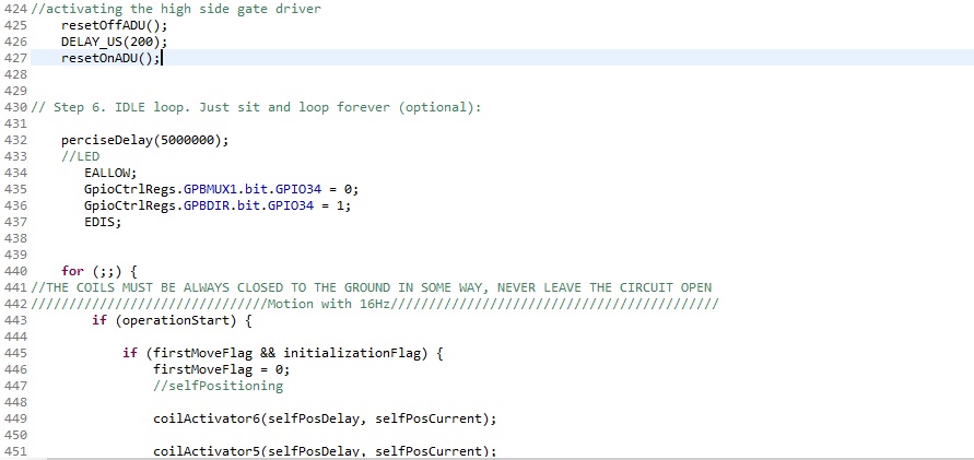
I can run the code up to "resetOffADU();" function and then the code goes in illegal ISR, when I comment this function, still inside the forever loop I again get stuck in other functions for timing and etc.

the "resetOffADU();" function is just a simple GPIO pin setting.

These are also some suspicious warnings which I'm receiving:


This is the first time that I face a problem in Texas microcontrollers which is such complicated and there aren't proper and solid documentations for that, I highly appreciate if you can lead me to the solution.

  • Not sure which version of ControlSuite you are using (that recommends SDFlash). I recommend you download the most recent version of c2000ware and use the linker command files provided in there as a starting point. As to your question "I want to know how can I verify in code composer that I'm assigning right memory parts /functions to RAM or Flash memories ", if you use the linker command file from c2000ware, it has all the right assignments for the "standard" sections. For any user defined section, the choice of loading a section in RAM or flash (or loading it in flash but copying it to RAM upon booting) is completely up to you.

    As to the warnings, it appears there are some sections defined in your code that do not have an assignment in the linker command file.

    Please take a look at the following posts:
    e2e.ti.com/.../839258 constants in RAM#839258

    e2e.ti.com/.../186266

  • Thanks for the reply, based on your recommendation I used C2000 ware linker commands. By progressing the testings I realized that the main cause of halting my code in some functions is ADC ISR, I mean whenever I deactivate the ADC ISR the whole code works fine, but when I activate the ADC ISR, the code inside the forever loop gets stuck in the first function! (in Flashing Mode not the RAM mode)

    The steps I'm doing to initialize flash is the following :

    1- defining the flash assignments:

    #include "DSP28x_Project.h"     // Device Headerfile and Examples Include File
    #include "DCL.h"
    #include "string.h"
    
    
    // Functions that will be run from RAM need to be assigned to
    // a different section.  This section will then be mapped using
    // the linker cmd file.
    //
    #pragma CODE_SECTION(epwm1_isr, "ramfuncs");
    #pragma CODE_SECTION(adc_isr, "ramfuncs");
    #pragma CODE_SECTION(cpu_timer0_isr, "ramfuncs");
    //#pragma CODE_SECTION(DCL_runPI, "ramfuncs");
    // These are defined by the linker (see F2808.cmd)
    //
    extern Uint16 RamfuncsLoadStart;
    extern Uint16 RamfuncsLoadEnd;
    extern Uint16 RamfuncsRunStart;
    extern Uint16 RamfuncsLoadSize;

    2- activating the interrupts and forever loop:

    void main(void) {


        // Copy time critical code and Flash setup code to RAM
        // This includes the following ISR functions: epwm1_timer_isr(),
        // epwm2_timer_isr(), epwm3_timer_isr and and InitFlash();
        // The  RamfuncsLoadStart, RamfuncsLoadSize, and RamfuncsRunStart
        // symbols are created by the linker. Refer to the F2808.cmd file.
        //
        memcpy(&RamfuncsRunStart, &RamfuncsLoadStart, (Uint32)&RamfuncsLoadSize);
    
    // Step 1. Initialize System Control:
    // PLL, WatchDog, enable Peripheral Clocks
    // This example function is found in the F2806x_SysCtrl.c file.
    
    
    	InitSysCtrl();
    
    
    // Step 2. Initalize GPIO:
    // This example function is found in the F2806x_Gpio.c file and
    // illustrates how to set the GPIO to it's default state.
    // InitGpio();  // Skipped for this example
    
    // For this case just init GPIO pins for ePWM1, ePWM2, ePWM3
    // These functions are in the F2806x_EPwm.c file
    	InitEPwm1Gpio();
    	//initialization of SCI GPIO
    	InitSciGpio();
    // Step 3. Clear all interrupts and initialize PIE vector table:
    // Disable CPU interrupts
    	DINT;
    
    // Initialize the PIE control registers to their default state.
    // The default state is all PIE interrupts disabled and flags
    // are cleared.
    // This function is found in the F2806x_PieCtrl.c file.
    	InitPieCtrl();
    
    // Disable CPU interrupts and clear all CPU interrupt flags:
    	IER = 0x0000;
    	IFR = 0x0000;
    
    // Initialize the PIE vector table with pointers to the shell Interrupt
    // Service Routines (ISR).
    // This will populate the entire table, even if the interrupt
    // is not used in this example.  This is useful for debug purposes.
    // The shell ISR routines are found in F2806x_DefaultIsr.c.
    // This function is found in F2806x_PieVect.c.
    	InitPieVectTable();
    
    // Interrupts that are used in this example are re-mapped to
    // ISR functions found within this file.
    	EALLOW;
    	PieVectTable.EPWM1_INT = &epwm1_isr;		//epwm1 interrupt
    	PieVectTable.ADCINT1 = &adc_isr;			//adc interrupt
    	PieVectTable.TINT0 = &cpu_timer0_isr;		//cpu timer interrup
    	PieVectTable.SCIRXINTA = &sciaRxFifoIsr;	//sci RX interrupt
    	//PieVectTable.SCITXINTA = &sciaTxFifoIsr;	//sci TX interrupt
    	EDIS;


        //
        // Call Flash Initialization to setup flash waitstates
        // This function must reside in RAM
        //
        InitFlash();
    
    // Step 4. Initialize all the Device Peripherals:
    // This function is found in F2806x_InitPeripherals.c
    // InitPeripherals();  // Not required for this example
    
    	InitAdc();  		//init the ADC
    	AdcOffsetSelfCal();
    	InitCpuTimers();  	//init the CPU timers
    	scia_fifo_init();  	// Init the SCI-A
    
    	// Configure CPU-Timer 0 to interrupt every micro-second:
    	// 90MHz CPU Freq, Period (in uSeconds), so as it mentioned it's based on the period of interrupts, sor for
    	//accurate timing the delay should be divided by 2 inorder to have right timings.
    	ConfigCpuTimer(&CpuTimer0, 90, 1);
    	// To ensure precise timing, use write-only instructions to write to the entire register. Therefore, if any
    	// of the configuration bits are changed in ConfigCpuTimer and InitCpuTimers (in F2806x_CpuTimers.h), the
    	// below settings must also be updated.
    	CpuTimer0Regs.TCR.all = 0x4000; // Use write-only instruction to set TSS bit = 0
    
    // For this example, only initialize the ePWM
    
    	EALLOW;
    	SysCtrlRegs.PCLKCR0.bit.TBCLKSYNC = 0;
    	EDIS;
    	//intialization of EPWM1 clocking and frequency
    	EPWM1init();
    
    	EALLOW;
    	SysCtrlRegs.PCLKCR0.bit.TBCLKSYNC = 1;
    	EDIS;
    
    	/***********************************************ADC*************************************************************************/
    	LoopCount = 0;
    	ConversionCount = 0;
    
    	// Configure ADC
    	EALLOW;
    	AdcRegs.ADCCTL2.bit.ADCNONOVERLAP = 1;	// Enable non-overlap mode
    	AdcRegs.ADCCTL1.bit.INTPULSEPOS = 1;// ADCINT1 trips after AdcResults latch
    	AdcRegs.INTSEL1N2.bit.INT1E = 1;	// Enabled ADCINT1
    	AdcRegs.INTSEL1N2.bit.INT1CONT = 0;	// Disable ADCINT1 Continuous mode
    	AdcRegs.INTSEL1N2.bit.INT1SEL = 1;  // setup EOC1 to trigger ADCINT1 to fire
    	AdcRegs.ADCSOC0CTL.bit.CHSEL = 4;    // set SOC0 channel select to ADCINA4
    	AdcRegs.ADCSOC1CTL.bit.CHSEL = 2;    // set SOC1 channel select to ADCINA2
    	AdcRegs.ADCSOC0CTL.bit.TRIGSEL = 5; // set SOC0 start trigger on EPWM1A, due to round-robin SOC0 converts first then SOC1
    	AdcRegs.ADCSOC1CTL.bit.TRIGSEL = 5; // set SOC1 start trigger on EPWM1A, due to round-robin SOC0 converts first then SOC1
    	AdcRegs.ADCSOC0CTL.bit.ACQPS = 6; // set SOC0 S/H Window to 7 ADC Clock Cycles, (6 ACQPS plus 1)
    	AdcRegs.ADCSOC1CTL.bit.ACQPS = 6; // set SOC1 S/H Window to 7 ADC Clock Cycles, (6 ACQPS plus 1)
    	EDIS;
    
    	// Assumes ePWM1 clock is already enabled in InitSysCtrl();
    	EPwm1Regs.ETSEL.bit.SOCAEN = 1;		// Enable SOC on A group
    	EPwm1Regs.ETSEL.bit.SOCASEL = 4;		// Select SOC from CMPA on upcount
    	EPwm1Regs.ETPS.bit.SOCAPRD = 1;		// Generate pulse on 1st event
    
    	/************************************************************************************************************************/
    	/*_____________________________PI controller initialization_____________________________*/
    	pi1.Umax = EPWM1_MAX_CMPA;
    	pi1.Umin = 0;
    	pi1.Kp = piKP;
    	pi1.Ki = piKI;
    	/*_______________________________________________________________________________________*/
    
    // Step 5. User specific code, enable interrupts:
    // Enable CPU INT3 which is connected to EPWM1-3 INT:
    	IER |= M_INT3;
    // Enable EPWM1 INTn in the PIE: Group 3 interrupt 1-3
    	PieCtrlRegs.PIEIER3.bit.INTx1 = 1;
    
    	// Enable ADCINT1 in PIE
    	PieCtrlRegs.PIEIER1.bit.INTx1 = 1;	// Enable INT 1.1 in the PIE (ADCINT1)
    
    	// Enable TINT0 in the PIE: Group 1 interrupt 7 For CPU Timer
    	PieCtrlRegs.PIEIER1.bit.INTx7 = 1;
    
    	IER |= M_INT1; 						// Enable CPU Interrupt 1
    
    	//Enabling the interrupt for SCIa
    	//PieCtrlRegs.PIECTRL.bit.ENPIE = 1;   	// Enable the PIE block
    	PieCtrlRegs.PIEIER9.bit.INTx1 = 1;      // PIE Group 9, INT1
    	//PieCtrlRegs.PIEIER9.bit.INTx2 = 1;      // PIE Group 9, INT2
    	IER |= M_INT9; 							// Enable CPU INT9 for SCIA
    
    
    	EINT;
    	// Enable Global interrupt INTM
    	ERTM;
    	// Enable Global realtime interrupt DBGM
    
    	resetOffADU();
    //	DELAY_US(200);
    	resetOnADU();
    
    
    /*// Step 6. IDLE loop. Just sit and loop forever (optional):
        EALLOW;
        GpioCtrlRegs.GPBMUX1.bit.GPIO34 = 0;
        GpioCtrlRegs.GPBDIR.bit.GPIO34 = 1;
        EDIS;*/
    
    
        perciseDelay(delayT);
    
    	for (;;) {
    
    		if (operationStart) {
    
    			if (firstMoveFlag && initializationFlag) {
    				firstMoveFlag = 0;
    				//selfPositioning
    
    				coilActivator6(selfPosDelay, selfPosCurrent);
    
    				coilActivator5(selfPosDelay, selfPosCurrent);
    
    				coilActivator4(selfPosDelay, selfPosCurrent);
    
    				coilActivator3(selfPosDelay, selfPosCurrent);
    
    				coilActivator2(selfPosDelay, selfPosCurrent);
    
    				coilActivator1(selfPosDelay, selfPosCurrent);
    
    				coilActivator1(delayCS1, 30.0);
    				coilActivator2(delayCS2, 30.0);
    				coilActivator3(delayCS3, 30.0);
    				coilActivator4(delayCS4, 30.0);
    				coilActivator5(delayCS5, 30.0);
    				coilActivator6(delayCS6, 30.0);
    
    			}
    }
    

    then the ADC ISR will be like :

    __interrupt void adc_isr(void) {
    
    	//Voltage1[ConversionCount] = AdcResult.ADCRESULT0;
    	Voltage2[ConversionCount] = AdcResult.ADCRESULT1;
    
    	if (firstFlag)
    		sampleNo = 5000;
    	else {
    		firstFlag = 0;
    		sampleNo = 5;
    	}
    	// If 100 conversions have been logged, start over
    	if (ConversionCount == sampleNo) {
    		int i = 0;
    		for (i = 0; i <= sampleNo - 1; i++) {
    			averageVoltage2 += Voltage2[i];
    		}
    		//averaging on a window of size 10
    		averageVoltage2 /= sampleNo;
    		//calculation of real value of the voltage
    		averageVoltage2 = 3.3 * averageVoltage2 / 4096.0 - voltageOffset;
    		if (averageVoltage2 < 0)
    			averageVoltage2 = 0;
    
    		//calculation of the real value of the current passing through the circuit
    		inputCurr = (averageVoltage2 - 0.00552) / 0.04928 - currentOffset;
    		//RMS value
    		//inputCurr*=0.7;
    
    		if (inputCurr < 0)
    			inputCurr = 0;
    
    		if (firstFlag) {
    			firstFlag = 0;
    			voltageOffset = averageVoltage2;
    			currentOffset = inputCurr;
    		}
    
    		ConversionCount = 0;
    	} else
    		ConversionCount++;
    
    	AdcRegs.ADCINTFLGCLR.bit.ADCINT1 = 1;//Clear ADCINT1 flag reinitialize for next SOC
    	PieCtrlRegs.PIEACK.all = PIEACK_GROUP1;   // Acknowledge interrupt to PIE
    
    	return;
    }

    Also it worth mentioning that the ADC is triggered by a PWM interrupt which contains inside a PI controller using Digital controller library:

    __interrupt void epwm1_isr(void) {
    	// Update the CMPA and CMPB values
    	//update_compare(&epwm1_info);
    
    	//controller running
    	uk = DCL_runPI(&pi1, rk, inputCurr);
    	x = (long) (uk);
    	z = (unsigned int) (x);
    
    	//setting the proper value for the DutyCycle based on the controller output
    	EPwm1Regs.CMPA.half.CMPA = z;
    	//EPwm1Regs.CMPA.half.CMPA=20;
    	// Clear INT flag for this timer
    	EPwm1Regs.ETCLR.bit.INT = 1;
    
    	// Acknowledge this interrupt to receive more interrupts from group 3
    	PieCtrlRegs.PIEACK.all = PIEACK_GROUP3;
    }

    So when I try to debug my code line by line, when the ADC interrupt is activated I get stuck in the first function in forever-loop which simply contains a delay inside written using "cpu_timer0_isr" (Not the Delay_us). I'm pretty sure that the error is due to the ADC functionality. I also read the following thread but still my problem persist.

    This is the 4th day which I'm stuck in flashing my code inside the microcontroller and I highly appreciate any help to solve this issue. 
    Regards

    Milad

    void main(void) {


        // Copy time critical code and Flash setup code to RAM    // This includes the following ISR functions: epwm1_timer_isr(),    // epwm2_timer_isr(), epwm3_timer_isr and and InitFlash();    // The  RamfuncsLoadStart, RamfuncsLoadSize, and RamfuncsRunStart    // symbols are created by the linker. Refer to the F2808.cmd file.    //    memcpy(&RamfuncsRunStart, &RamfuncsLoadStart, (Uint32)&RamfuncsLoadSize);
    // Step 1. Initialize System Control:// PLL, WatchDog, enable Peripheral Clocks// This example function is found in the F2806x_SysCtrl.c file.

    InitSysCtrl();

    // Step 2. Initalize GPIO:// This example function is found in the F2806x_Gpio.c file and// illustrates how to set the GPIO to it's default state.// InitGpio();  // Skipped for this example
    // For this case just init GPIO pins for ePWM1, ePWM2, ePWM3// These functions are in the F2806x_EPwm.c file InitEPwm1Gpio(); //initialization of SCI GPIO InitSciGpio();// Step 3. Clear all interrupts and initialize PIE vector table:// Disable CPU interrupts DINT;
    // Initialize the PIE control registers to their default state.// The default state is all PIE interrupts disabled and flags// are cleared.// This function is found in the F2806x_PieCtrl.c file. InitPieCtrl();
    // Disable CPU interrupts and clear all CPU interrupt flags: IER = 0x0000; IFR = 0x0000;
    // Initialize the PIE vector table with pointers to the shell Interrupt// Service Routines (ISR).// This will populate the entire table, even if the interrupt// is not used in this example.  This is useful for debug purposes.// The shell ISR routines are found in F2806x_DefaultIsr.c.// This function is found in F2806x_PieVect.c. InitPieVectTable();
    // Interrupts that are used in this example are re-mapped to// ISR functions found within this file. EALLOW; PieVectTable.EPWM1_INT = &epwm1_isr; //epwm1 interrupt PieVectTable.ADCINT1 = &adc_isr; //adc interrupt PieVectTable.TINT0 = &cpu_timer0_isr; //cpu timer interrup PieVectTable.SCIRXINTA = &sciaRxFifoIsr; //sci RX interrupt //PieVectTable.SCITXINTA = &sciaTxFifoIsr; //sci TX interrupt EDIS;


        //    // Call Flash Initialization to setup flash waitstates    // This function must reside in RAM    //    InitFlash();
    // Step 4. Initialize all the Device Peripherals:// This function is found in F2806x_InitPeripherals.c// InitPeripherals();  // Not required for this example
    InitAdc();  //init the ADC AdcOffsetSelfCal(); InitCpuTimers();  //init the CPU timers scia_fifo_init();  // Init the SCI-A
    // Configure CPU-Timer 0 to interrupt every micro-second: // 90MHz CPU Freq, Period (in uSeconds), so as it mentioned it's based on the period of interrupts, sor for //accurate timing the delay should be divided by 2 inorder to have right timings. ConfigCpuTimer(&CpuTimer0, 90, 1); // To ensure precise timing, use write-only instructions to write to the entire register. Therefore, if any // of the configuration bits are changed in ConfigCpuTimer and InitCpuTimers (in F2806x_CpuTimers.h), the // below settings must also be updated. CpuTimer0Regs.TCR.all = 0x4000; // Use write-only instruction to set TSS bit = 0
    // For this example, only initialize the ePWM
    EALLOW; SysCtrlRegs.PCLKCR0.bit.TBCLKSYNC = 0; EDIS; //intialization of EPWM1 clocking and frequency EPWM1init();
    EALLOW; SysCtrlRegs.PCLKCR0.bit.TBCLKSYNC = 1; EDIS;
    /***********************************************ADC*************************************************************************/ LoopCount = 0; ConversionCount = 0;
    // Configure ADC EALLOW; AdcRegs.ADCCTL2.bit.ADCNONOVERLAP = 1; // Enable non-overlap mode AdcRegs.ADCCTL1.bit.INTPULSEPOS = 1;// ADCINT1 trips after AdcResults latch AdcRegs.INTSEL1N2.bit.INT1E = 1; // Enabled ADCINT1 AdcRegs.INTSEL1N2.bit.INT1CONT = 0; // Disable ADCINT1 Continuous mode AdcRegs.INTSEL1N2.bit.INT1SEL = 1;  // setup EOC1 to trigger ADCINT1 to fire AdcRegs.ADCSOC0CTL.bit.CHSEL = 4;    // set SOC0 channel select to ADCINA4 AdcRegs.ADCSOC1CTL.bit.CHSEL = 2;    // set SOC1 channel select to ADCINA2 AdcRegs.ADCSOC0CTL.bit.TRIGSEL = 5; // set SOC0 start trigger on EPWM1A, due to round-robin SOC0 converts first then SOC1 AdcRegs.ADCSOC1CTL.bit.TRIGSEL = 5; // set SOC1 start trigger on EPWM1A, due to round-robin SOC0 converts first then SOC1 AdcRegs.ADCSOC0CTL.bit.ACQPS = 6; // set SOC0 S/H Window to 7 ADC Clock Cycles, (6 ACQPS plus 1) AdcRegs.ADCSOC1CTL.bit.ACQPS = 6; // set SOC1 S/H Window to 7 ADC Clock Cycles, (6 ACQPS plus 1) EDIS;
    // Assumes ePWM1 clock is already enabled in InitSysCtrl(); EPwm1Regs.ETSEL.bit.SOCAEN = 1; // Enable SOC on A group EPwm1Regs.ETSEL.bit.SOCASEL = 4; // Select SOC from CMPA on upcount EPwm1Regs.ETPS.bit.SOCAPRD = 1; // Generate pulse on 1st event
    /************************************************************************************************************************/ /*_____________________________PI controller initialization_____________________________*/ pi1.Umax = EPWM1_MAX_CMPA; pi1.Umin = 0; pi1.Kp = piKP; pi1.Ki = piKI; /*_______________________________________________________________________________________*///activating the high side gate driver resetGPIOinit();//initialization of the coil selector GPIO coilSelectorInitGPIO();
    // Step 5. User specific code, enable interrupts:// Enable CPU INT3 which is connected to EPWM1-3 INT: IER |= M_INT3;// Enable EPWM1 INTn in the PIE: Group 3 interrupt 1-3 PieCtrlRegs.PIEIER3.bit.INTx1 = 1;
    // Enable ADCINT1 in PIE PieCtrlRegs.PIEIER1.bit.INTx1 = 1; // Enable INT 1.1 in the PIE (ADCINT1)
    // Enable TINT0 in the PIE: Group 1 interrupt 7 For CPU Timer PieCtrlRegs.PIEIER1.bit.INTx7 = 1;
    IER |= M_INT1; // Enable CPU Interrupt 1
    //Enabling the interrupt for SCIa //PieCtrlRegs.PIECTRL.bit.ENPIE = 1;    // Enable the PIE block PieCtrlRegs.PIEIER9.bit.INTx1 = 1;      // PIE Group 9, INT1 //PieCtrlRegs.PIEIER9.bit.INTx2 = 1;      // PIE Group 9, INT2 IER |= M_INT9; // Enable CPU INT9 for SCIA

    EINT; // Enable Global interrupt INTM ERTM; // Enable Global realtime interrupt DBGM
    resetOffADU();// DELAY_US(200); resetOnADU();

    /*// Step 6. IDLE loop. Just sit and loop forever (optional):    EALLOW;    GpioCtrlRegs.GPBMUX1.bit.GPIO34 = 0;    GpioCtrlRegs.GPBDIR.bit.GPIO34 = 1;    EDIS;*/

        perciseDelay(delayT);
    for (;;) {//THE COILS MUST BE ALWAYS CLOSED TO THE GROUND IN SOME WAY, NEVER LEAVE THE CIRCUIT OPEN///////////////////////////////Motion with 16Hz/////////////////////////////////////////// if (operationStart) {
    if (firstMoveFlag && initializationFlag) { firstMoveFlag = 0; //selfPositioning
    coilActivator6(selfPosDelay, selfPosCurrent);
    coilActivator5(selfPosDelay, selfPosCurrent);
    coilActivator4(selfPosDelay, selfPosCurrent);
    coilActivator3(selfPosDelay, selfPosCurrent);
    coilActivator2(selfPosDelay, selfPosCurrent);
    coilActivator1(selfPosDelay, selfPosCurrent);
    //shooting coilActivator1(delayCS1, 30.0); coilActivator2(delayCS2, 30.0); coilActivator3(delayCS3, 30.0); coilActivator4(delayCS4, 30.0); coilActivator5(delayCS5, 30.0); coilActivator6(delayCS6, 30.0);
    }

  • If you have isolated the ADC interrupt as the problem (that too when run from RAM), you could whittle down the ADC ISR and progressively add code to isolate the issue.

  • Yes, but When I run from RAM there is no problem, the whole system works like a charm, but when I move to flash the ADC interrupt gets bugged, The thing is I'm using Cpu timer0 interrupt also, so I'm not sure when we are flashing should I consider some modifications for that or not ( I mean the way of acknowledging the interrupts or sth like that).
  • Hi,

    Your application fits in RAM and your toolchain has an RTS lib that can take care of copying all of your code in RAM before calling the main() function, just like your debugger in the RAM model. This way your code should work just like before.

    Please check this:

    Project right click/Properties/Build/C2000 Compiler/Advanced Options/Runtime Model Options/--ramfunc = on

    Linker script fragment:

    GROUP
         {
           	.TI.ramfunc
            {
             	-l F021_API_CortexM3_LE.lib (.text)
           	}
         }	LOAD = APP_FLASH,
    		RUN = APP_RAM,
    		PALIGN(0x10),
    		TABLE(BINIT),
    		PAGE = 0
    
        .binit : palign=0x8, fill=0xffff > APP_FLASH

    All CODE_SECTION pragmas and the memcpy should be gone...

    Regards,

    Janos

  • Thanks Janos for your very helpful reply, 

    I tried your method but when I modify my F28069M.cmd file like how you've suggested I get some errors. 

    I think the example you've shared for the linker command file is for another microcontroller, so the compiler can not recognize some parts of it.

    I took the simpler section from the link you've shared, but still I receive errors. The thing is inside the section part what should I put instead of Flash and RAM??? Because there are other sections defined with different names like RAML0 or etc, also in your code segment APP_RAM is not defined in my cmd file. I've attached my cmd file here.?

    .TI.ramfunc : {} load=FLASH, run=RAM, table(BINIT)
    
     .binit : {} > FLASH

    The errors I receive:


    F28069.txt
    /*
    //###########################################################################
    //
    // FILE:    F28069.cmd
    //
    // TITLE:   Linker Command File For F28069 Device
    //
    //###########################################################################
    // $TI Release: F2806x C/C++ Header Files and Peripheral Examples V150 $
    // $Release Date: June 16, 2015 $
    // $Copyright: Copyright (C) 2011-2015 Texas Instruments Incorporated -
    //             http://www.ti.com/ ALL RIGHTS RESERVED $
    //###########################################################################
    */
    
    /* ======================================================
    // For Code Composer Studio V2.2 and later
    // ---------------------------------------
    // In addition to this memory linker command file,
    // add the header linker command file directly to the project.
    // The header linker command file is required to link the
    // peripheral structures to the proper locations within
    // the memory map.
    //
    // The header linker files are found in <base>\F2806x_headers\cmd
    //
    // For BIOS applications add:      F2806x_Headers_BIOS.cmd
    // For nonBIOS applications add:   F2806x_Headers_nonBIOS.cmd
    ========================================================= */
    
    /* ======================================================
    // For Code Composer Studio prior to V2.2
    // --------------------------------------
    // 1) Use one of the following -l statements to include the
    // header linker command file in the project. The header linker
    // file is required to link the peripheral structures to the proper
    // locations within the memory map                                    */
    
    /* Uncomment this line to include file only for non-BIOS applications */
    /* -l F2806x_Headers_nonBIOS.cmd */
    
    /* Uncomment this line to include file only for BIOS applications */
    /* -l F2806x_Headers_BIOS.cmd */
    
    /* 2) In your project add the path to <base>\F2806x_headers\cmd to the
       library search path under project->build options, linker tab,
       library search path (-i).
    /*========================================================= */
    
    /* Define the memory block start/length for the F2806x
       PAGE 0 will be used to organize program sections
       PAGE 1 will be used to organize data sections
    
       Notes:
             Memory blocks on F28069 are uniform (ie same
             physical memory) in both PAGE 0 and PAGE 1.
             That is the same memory region should not be
             defined for both PAGE 0 and PAGE 1.
             Doing so will result in corruption of program
             and/or data.
    
             Contiguous SARAM memory blocks can be combined
             if required to create a larger memory block.
    */
    
    MEMORY
    {
    PAGE 0 :   /* Program Memory */
               /* Memory (RAM/FLASH/OTP) blocks can be moved to PAGE1 for data allocation */
       RAML0       : origin = 0x008000, length = 0x000800     /* on-chip RAM block L0 */
       RAML1       : origin = 0x008800, length = 0x000400     /* on-chip RAM block L1 */
       OTP         : origin = 0x3D7800, length = 0x000400     /* on-chip OTP */
    
       FLASHH      : origin = 0x3D8000, length = 0x004000     /* on-chip FLASH */
       FLASHG      : origin = 0x3DC000, length = 0x004000     /* on-chip FLASH */
       FLASHF      : origin = 0x3E0000, length = 0x004000     /* on-chip FLASH */
       FLASHE      : origin = 0x3E4000, length = 0x004000     /* on-chip FLASH */   
       FLASHD      : origin = 0x3E8000, length = 0x004000     /* on-chip FLASH */
       FLASHC      : origin = 0x3EC000, length = 0x004000     /* on-chip FLASH */
       FLASHA      : origin = 0x3F4000, length = 0x003F80     /* on-chip FLASH */
       CSM_RSVD    : origin = 0x3F7F80, length = 0x000076     /* Part of FLASHA.  Program with all 0x0000 when CSM is in use. */
       BEGIN       : origin = 0x3F7FF6, length = 0x000002     /* Part of FLASHA.  Used for "boot to Flash" bootloader mode. */
       CSM_PWL_P0  : origin = 0x3F7FF8, length = 0x000008     /* Part of FLASHA.  CSM password locations in FLASHA */
    
       FPUTABLES   : origin = 0x3FD860, length = 0x0006A0	  /* FPU Tables in Boot ROM */
       IQTABLES    : origin = 0x3FDF00, length = 0x000B50     /* IQ Math Tables in Boot ROM */
       IQTABLES2   : origin = 0x3FEA50, length = 0x00008C     /* IQ Math Tables in Boot ROM */
       IQTABLES3   : origin = 0x3FEADC, length = 0x0000AA	  /* IQ Math Tables in Boot ROM */
    
       ROM         : origin = 0x3FF3B0, length = 0x000C10     /* Boot ROM */
       RESET       : origin = 0x3FFFC0, length = 0x000002     /* part of boot ROM  */
       VECTORS     : origin = 0x3FFFC2, length = 0x00003E     /* part of boot ROM  */
    
    PAGE 1 :   /* Data Memory */
               /* Memory (RAM/FLASH/OTP) blocks can be moved to PAGE0 for program allocation */
               /* Registers remain on PAGE1                                                  */
    
       BOOT_RSVD   : origin = 0x000000, length = 0x000050     /* Part of M0, BOOT rom will use this for stack */
       RAMM0       : origin = 0x000050, length = 0x0003B0     /* on-chip RAM block M0 */
       RAMM1       : origin = 0x000400, length = 0x000400     /* on-chip RAM block M1 */
       RAML2       : origin = 0x008C00, length = 0x000400     /* on-chip RAM block L2 */
       RAML3       : origin = 0x009000, length = 0x001000	  /* on-chip RAM block L3 */
       RAML4       : origin = 0x00A000, length = 0x002000     /* on-chip RAM block L4 */
       RAML5       : origin = 0x00C000, length = 0x002000     /* on-chip RAM block L5 */
       RAML6       : origin = 0x00E000, length = 0x002000     /* on-chip RAM block L6 */
       RAML7       : origin = 0x010000, length = 0x002000     /* on-chip RAM block L7 */
       RAML8       : origin = 0x012000, length = 0x002000     /* on-chip RAM block L8 */
       USB_RAM     : origin = 0x040000, length = 0x000800     /* USB RAM		  */   
       FLASHB      : origin = 0x3F0000, length = 0x004000     /* on-chip FLASH */     
    }
    
    /* Allocate sections to memory blocks.
       Note:
             codestart user defined section in DSP28_CodeStartBranch.asm used to redirect code
                       execution when booting to flash
             ramfuncs  user defined section to store functions that will be copied from Flash into RAM
    */
    
    
    SECTIONS
    {
     .TI.ramfunc : {} load=FLASH, run=RAM, table(BINIT)
      .binit : {} > FLASH
      
       /* Allocate program areas: */
       .cinit              : > FLASHA,     PAGE = 0
       .pinit              : > FLASHA,     PAGE = 0
       .text               : > FLASHA,     PAGE = 0
       codestart           : > BEGIN,      PAGE = 0
       ramfuncs            : LOAD = FLASHD,
                             RUN = RAML0,
                             LOAD_START(_RamfuncsLoadStart),
                             LOAD_END(_RamfuncsLoadEnd),
                             RUN_START(_RamfuncsRunStart),
    						 LOAD_SIZE(_RamfuncsLoadSize),
                             PAGE = 0
    
       csmpasswds          : > CSM_PWL_P0, PAGE = 0
       csm_rsvd            : > CSM_RSVD,   PAGE = 0
    
       /* Allocate uninitalized data sections: */
       .stack              : > RAMM0,      PAGE = 1
       .ebss               : > RAML2,      PAGE = 1
       .esysmem            : > RAML2,      PAGE = 1
    
       /* Initalized sections to go in Flash */
       /* For SDFlash to program these, they must be allocated to page 0 */
       .econst             : > FLASHA,     PAGE = 0
       .switch             : > FLASHA,     PAGE = 0
    
       /* Allocate IQ math areas: */
       IQmath              : > FLASHA,     PAGE = 0            /* Math Code */
       IQmathTables        : > IQTABLES,   PAGE = 0, TYPE = NOLOAD
       
       /* Allocate FPU math areas: */
       FPUmathTables       : > FPUTABLES,  PAGE = 0, TYPE = NOLOAD
       
       DMARAML5	           : > RAML5,      PAGE = 1
       DMARAML6	           : > RAML6,      PAGE = 1
       DMARAML7	           : > RAML7,      PAGE = 1
       DMARAML8	           : > RAML8,      PAGE = 1   
    
      /* Uncomment the section below if calling the IQNexp() or IQexp()
          functions from the IQMath.lib library in order to utilize the
          relevant IQ Math table in Boot ROM (This saves space and Boot ROM
          is 1 wait-state). If this section is not uncommented, IQmathTables2
          will be loaded into other memory (SARAM, Flash, etc.) and will take
          up space, but 0 wait-state is possible.
       */
       /*
       IQmathTables2    : > IQTABLES2, PAGE = 0, TYPE = NOLOAD
       {
    
                  IQmath.lib<IQNexpTable.obj> (IQmathTablesRam)
    
       }
       */
        /* Uncomment the section below if calling the IQNasin() or IQasin()
           functions from the IQMath.lib library in order to utilize the
           relevant IQ Math table in Boot ROM (This saves space and Boot ROM
           is 1 wait-state). If this section is not uncommented, IQmathTables2
           will be loaded into other memory (SARAM, Flash, etc.) and will take
           up space, but 0 wait-state is possible.
        */
        /*
        IQmathTables3    : > IQTABLES3, PAGE = 0, TYPE = NOLOAD
        {
    
                   IQmath.lib<IQNasinTable.obj> (IQmathTablesRam)
    
        }
        */
    
       /* .reset is a standard section used by the compiler.  It contains the */
       /* the address of the start of _c_int00 for C Code.   /*
       /* When using the boot ROM this section and the CPU vector */
       /* table is not needed.  Thus the default type is set here to  */
       /* DSECT  */
       .reset              : > RESET,      PAGE = 0, TYPE = DSECT
       vectors             : > VECTORS,    PAGE = 0, TYPE = DSECT
    
    }
    
    /*
    //===========================================================================
    // End of file.
    //===========================================================================
    */


  • Hi,

    Basically the linker tries to find memory areas called FLASH and RAM, and neither were found in the linker script you attached to your post.

    I fixed up your linker command file, please find it attached.

    Regards,

    Janos

    3515.F28069.txt
    /*
    //###########################################################################
    //
    // FILE:    F28069.cmd
    //
    // TITLE:   Linker Command File For F28069 Device
    //
    //###########################################################################
    // $TI Release: F2806x C/C++ Header Files and Peripheral Examples V150 $
    // $Release Date: June 16, 2015 $
    // $Copyright: Copyright (C) 2011-2015 Texas Instruments Incorporated -
    //             http://www.ti.com/ ALL RIGHTS RESERVED $
    //###########################################################################
    */
    
    /* ======================================================
    // For Code Composer Studio V2.2 and later
    // ---------------------------------------
    // In addition to this memory linker command file,
    // add the header linker command file directly to the project.
    // The header linker command file is required to link the
    // peripheral structures to the proper locations within
    // the memory map.
    //
    // The header linker files are found in <base>\F2806x_headers\cmd
    //
    // For BIOS applications add:      F2806x_Headers_BIOS.cmd
    // For nonBIOS applications add:   F2806x_Headers_nonBIOS.cmd
    ========================================================= */
    
    /* ======================================================
    // For Code Composer Studio prior to V2.2
    // --------------------------------------
    // 1) Use one of the following -l statements to include the
    // header linker command file in the project. The header linker
    // file is required to link the peripheral structures to the proper
    // locations within the memory map                                    */
    
    /* Uncomment this line to include file only for non-BIOS applications */
    /* -l F2806x_Headers_nonBIOS.cmd */
    
    /* Uncomment this line to include file only for BIOS applications */
    /* -l F2806x_Headers_BIOS.cmd */
    
    /* 2) In your project add the path to <base>\F2806x_headers\cmd to the
       library search path under project->build options, linker tab,
       library search path (-i).
    /*========================================================= */
    
    /* Define the memory block start/length for the F2806x
       PAGE 0 will be used to organize program sections
       PAGE 1 will be used to organize data sections
    
       Notes:
             Memory blocks on F28069 are uniform (ie same
             physical memory) in both PAGE 0 and PAGE 1.
             That is the same memory region should not be
             defined for both PAGE 0 and PAGE 1.
             Doing so will result in corruption of program
             and/or data.
    
             Contiguous SARAM memory blocks can be combined
             if required to create a larger memory block.
    */
    
    MEMORY
    {
    PAGE 0 :   /* Program Memory */
               /* Memory (RAM/FLASH/OTP) blocks can be moved to PAGE1 for data allocation */
    /*
       RAML0       : origin = 0x008000, length = 0x000800
       RAML1       : origin = 0x008800, length = 0x000400
    */
    
       OTP         : origin = 0x3D7800, length = 0x000400     /* on-chip OTP */
    
    	FLASH		: origin = 0x3D8000, length = 0x018000
    	RAM			: origin = 0x008000, length = 0x00C000
    
    /*
       FLASHH      : origin = 0x3D8000, length = 0x004000
       FLASHG      : origin = 0x3DC000, length = 0x004000
       FLASHF      : origin = 0x3E0000, length = 0x004000
       FLASHE      : origin = 0x3E4000, length = 0x004000   
       FLASHD      : origin = 0x3E8000, length = 0x004000
       FLASHC      : origin = 0x3EC000, length = 0x004000
    */   
       
       FLASHA      : origin = 0x3F4000, length = 0x003F80     /* on-chip FLASH */
       CSM_RSVD    : origin = 0x3F7F80, length = 0x000076     /* Part of FLASHA.  Program with all 0x0000 when CSM is in use. */
       BEGIN       : origin = 0x3F7FF6, length = 0x000002     /* Part of FLASHA.  Used for "boot to Flash" bootloader mode. */
       CSM_PWL_P0  : origin = 0x3F7FF8, length = 0x000008     /* Part of FLASHA.  CSM password locations in FLASHA */
    
       FPUTABLES   : origin = 0x3FD860, length = 0x0006A0	  /* FPU Tables in Boot ROM */
       IQTABLES    : origin = 0x3FDF00, length = 0x000B50     /* IQ Math Tables in Boot ROM */
       IQTABLES2   : origin = 0x3FEA50, length = 0x00008C     /* IQ Math Tables in Boot ROM */
       IQTABLES3   : origin = 0x3FEADC, length = 0x0000AA	  /* IQ Math Tables in Boot ROM */
    
       ROM         : origin = 0x3FF3B0, length = 0x000C10     /* Boot ROM */
       RESET       : origin = 0x3FFFC0, length = 0x000002     /* part of boot ROM  */
       VECTORS     : origin = 0x3FFFC2, length = 0x00003E     /* part of boot ROM  */
    
    PAGE 1 :   /* Data Memory */
               /* Memory (RAM/FLASH/OTP) blocks can be moved to PAGE0 for program allocation */
               /* Registers remain on PAGE1                                                  */
    
    	SYSRAM			: origin = 0x000000, length = 0x000800
    
    /*
       BOOT_RSVD   : origin = 0x000000, length = 0x000050
       RAMM0       : origin = 0x000050, length = 0x0003B0
       RAMM1       : origin = 0x000400, length = 0x000400
    */
    
    	
    /*
       RAML2       : origin = 0x008C00, length = 0x000400
       RAML3       : origin = 0x009000, length = 0x001000
       RAML4       : origin = 0x00A000, length = 0x002000
       RAML5       : origin = 0x00C000, length = 0x002000
       RAML6       : origin = 0x00E000, length = 0x002000
       RAML7       : origin = 0x010000, length = 0x002000
       RAML8       : origin = 0x012000, length = 0x002000
    */
    
       USB_RAM     : origin = 0x040000, length = 0x000800     /* USB RAM		  */   
       FLASHB      : origin = 0x3F0000, length = 0x004000     /* on-chip FLASH */     
    }
    
    /* Allocate sections to memory blocks.
       Note:
             codestart user defined section in DSP28_CodeStartBranch.asm used to redirect code
                       execution when booting to flash
             ramfuncs  user defined section to store functions that will be copied from Flash into RAM
    */
    
    
    SECTIONS
    {
       /* Allocate program areas: */
       .cinit              : > FLASH,     PAGE = 0
       .pinit              : > FLASH,     PAGE = 0
       .text               : > FLASH,     PAGE = 0
       codestart           : > BEGIN,      PAGE = 0
    /*
       ramfuncs            : LOAD = FLASHD,
                             RUN = RAML0,
                             LOAD_START(_RamfuncsLoadStart),
                             LOAD_END(_RamfuncsLoadEnd),
                             RUN_START(_RamfuncsRunStart),
    						 LOAD_SIZE(_RamfuncsLoadSize),
                             PAGE = 0
    */
       csmpasswds          : > CSM_PWL_P0, PAGE = 0
       csm_rsvd            : > CSM_RSVD,   PAGE = 0
    
       /* Allocate uninitalized data sections: */
       .stack              : > SYSRAM,      PAGE = 1
       .ebss               : > RAM,      PAGE = 1
       .esysmem            : > RAM,      PAGE = 1
    
       /* Initalized sections to go in Flash */
       /* For SDFlash to program these, they must be allocated to page 0 */
       .econst             : > FLASH,     PAGE = 0
       .switch             : > FLASH,     PAGE = 0
       
       GROUP
        {
        	.TI.ramfunc
        	ramfuncs
        	{
        	}
        }    LOAD = FLASH,
             RUN = RAM,
             PAGE = 0,
             TABLE(BINIT)
    
       .binit : palign=0x8, fill=0xffff > FLASH
    
       /* Allocate IQ math areas: */
       IQmath              : > FLASH,     PAGE = 0            /* Math Code */
       IQmathTables        : > IQTABLES,   PAGE = 0, TYPE = NOLOAD
       
       /* Allocate FPU math areas: */
       FPUmathTables       : > FPUTABLES,  PAGE = 0, TYPE = NOLOAD
       
       /*
       DMARAML5	           : > RAML5,      PAGE = 1
       DMARAML6	           : > RAML6,      PAGE = 1
       DMARAML7	           : > RAML7,      PAGE = 1
       DMARAML8	           : > RAML8,      PAGE = 1
       */   
    
      /* Uncomment the section below if calling the IQNexp() or IQexp()
          functions from the IQMath.lib library in order to utilize the
          relevant IQ Math table in Boot ROM (This saves space and Boot ROM
          is 1 wait-state). If this section is not uncommented, IQmathTables2
          will be loaded into other memory (SARAM, Flash, etc.) and will take
          up space, but 0 wait-state is possible.
       */
       /*
       IQmathTables2    : > IQTABLES2, PAGE = 0, TYPE = NOLOAD
       {
    
                  IQmath.lib<IQNexpTable.obj> (IQmathTablesRam)
    
       }
       */
        /* Uncomment the section below if calling the IQNasin() or IQasin()
           functions from the IQMath.lib library in order to utilize the
           relevant IQ Math table in Boot ROM (This saves space and Boot ROM
           is 1 wait-state). If this section is not uncommented, IQmathTables2
           will be loaded into other memory (SARAM, Flash, etc.) and will take
           up space, but 0 wait-state is possible.
        */
        /*
        IQmathTables3    : > IQTABLES3, PAGE = 0, TYPE = NOLOAD
        {
    
                   IQmath.lib<IQNasinTable.obj> (IQmathTablesRam)
    
        }
        */
    
       /* .reset is a standard section used by the compiler.  It contains the */
       /* the address of the start of _c_int00 for C Code.   /*
       /* When using the boot ROM this section and the CPU vector */
       /* table is not needed.  Thus the default type is set here to  */
       /* DSECT  */
       .reset              : > RESET,      PAGE = 0, TYPE = DSECT
       vectors             : > VECTORS,    PAGE = 0, TYPE = DSECT
    
    }
    
    /*
    //===========================================================================
    // End of file.
    //===========================================================================
    */


  • Thanks a lot Janos for you modifications which they indeed helped alot. I think there were a slight error in your attached file assigning memory to the following part which I modified it my self:

    After this Modification I receive no Error, so simply what I did is I left the C code written for RAM unchanged, I just changed the linker command file as you recommended, Now when I run the system it seems very slow and I think the controller doesn't perform well.(The PI controller)

    I'm using Digital controller library and based on the assembly file for that, it's recommended to assign the memory like below:

        dclfuncs			   : > RAM,		   PAGE = 0
    

    but even after doing this the system runs slowly, also after flashing the .out file on my microcontroller and after power recycling the program doesn't start again. What is your opinion about the possible problems? ( I've attached the new cmd file)

    F28069M.txt
    /*
    //###########################################################################
    //
    // FILE:    F28069.cmd
    //
    // TITLE:   Linker Command File For F28069 Device
    //
    //###########################################################################
    // $TI Release: F2806x C/C++ Header Files and Peripheral Examples V150 $
    // $Release Date: June 16, 2015 $
    // $Copyright: Copyright (C) 2011-2015 Texas Instruments Incorporated -
    //             http://www.ti.com/ ALL RIGHTS RESERVED $
    //###########################################################################
    */
    
    /* ======================================================
    // For Code Composer Studio V2.2 and later
    // ---------------------------------------
    // In addition to this memory linker command file,
    // add the header linker command file directly to the project.
    // The header linker command file is required to link the
    // peripheral structures to the proper locations within
    // the memory map.
    //
    // The header linker files are found in <base>\F2806x_headers\cmd
    //
    // For BIOS applications add:      F2806x_Headers_BIOS.cmd
    // For nonBIOS applications add:   F2806x_Headers_nonBIOS.cmd
    ========================================================= */
    
    /* ======================================================
    // For Code Composer Studio prior to V2.2
    // --------------------------------------
    // 1) Use one of the following -l statements to include the
    // header linker command file in the project. The header linker
    // file is required to link the peripheral structures to the proper
    // locations within the memory map                                    */
    
    /* Uncomment this line to include file only for non-BIOS applications */
    /* -l F2806x_Headers_nonBIOS.cmd */
    
    /* Uncomment this line to include file only for BIOS applications */
    /* -l F2806x_Headers_BIOS.cmd */
    
    /* 2) In your project add the path to <base>\F2806x_headers\cmd to the
       library search path under project->build options, linker tab,
       library search path (-i).
    /*========================================================= */
    
    /* Define the memory block start/length for the F2806x
       PAGE 0 will be used to organize program sections
       PAGE 1 will be used to organize data sections
    
       Notes:
             Memory blocks on F28069 are uniform (ie same
             physical memory) in both PAGE 0 and PAGE 1.
             That is the same memory region should not be
             defined for both PAGE 0 and PAGE 1.
             Doing so will result in corruption of program
             and/or data.
    
             Contiguous SARAM memory blocks can be combined
             if required to create a larger memory block.
    */
    
    MEMORY
    {
    PAGE 0 :   /* Program Memory */
               /* Memory (RAM/FLASH/OTP) blocks can be moved to PAGE1 for data allocation */
    /*
       RAML0       : origin = 0x008000, length = 0x000800
       RAML1       : origin = 0x008800, length = 0x000400
    */
    
       OTP         : origin = 0x3D7800, length = 0x000400     /* on-chip OTP */
    
    	FLASH		: origin = 0x3D8000, length = 0x018000
    	RAM			: origin = 0x008000, length = 0x00C000
    
    /*
       FLASHH      : origin = 0x3D8000, length = 0x004000
       FLASHG      : origin = 0x3DC000, length = 0x004000
       FLASHF      : origin = 0x3E0000, length = 0x004000
       FLASHE      : origin = 0x3E4000, length = 0x004000
       FLASHD      : origin = 0x3E8000, length = 0x004000
       FLASHC      : origin = 0x3EC000, length = 0x004000
    */
    
       FLASHA      : origin = 0x3F4000, length = 0x003F80     /* on-chip FLASH */
       CSM_RSVD    : origin = 0x3F7F80, length = 0x000076     /* Part of FLASHA.  Program with all 0x0000 when CSM is in use. */
       BEGIN       : origin = 0x3F7FF6, length = 0x000002     /* Part of FLASHA.  Used for "boot to Flash" bootloader mode. */
       CSM_PWL_P0  : origin = 0x3F7FF8, length = 0x000008     /* Part of FLASHA.  CSM password locations in FLASHA */
    
       FPUTABLES   : origin = 0x3FD860, length = 0x0006A0	  /* FPU Tables in Boot ROM */
       IQTABLES    : origin = 0x3FDF00, length = 0x000B50     /* IQ Math Tables in Boot ROM */
       IQTABLES2   : origin = 0x3FEA50, length = 0x00008C     /* IQ Math Tables in Boot ROM */
       IQTABLES3   : origin = 0x3FEADC, length = 0x0000AA	  /* IQ Math Tables in Boot ROM */
    
       ROM         : origin = 0x3FF3B0, length = 0x000C10     /* Boot ROM */
       RESET       : origin = 0x3FFFC0, length = 0x000002     /* part of boot ROM  */
       VECTORS     : origin = 0x3FFFC2, length = 0x00003E     /* part of boot ROM  */
    
    PAGE 1 :   /* Data Memory */
               /* Memory (RAM/FLASH/OTP) blocks can be moved to PAGE0 for program allocation */
               /* Registers remain on PAGE1                                                  */
    
    	SYSRAM			: origin = 0x000000, length = 0x000800
    
    /*
       BOOT_RSVD   : origin = 0x000000, length = 0x000050
       RAMM0       : origin = 0x000050, length = 0x0003B0
       RAMM1       : origin = 0x000400, length = 0x000400
    */
    
    
    /*
       RAML2       : origin = 0x008C00, length = 0x000400
       RAML3       : origin = 0x009000, length = 0x001000
       RAML4       : origin = 0x00A000, length = 0x002000
       RAML5       : origin = 0x00C000, length = 0x002000
       RAML6       : origin = 0x00E000, length = 0x002000
       RAML7       : origin = 0x010000, length = 0x002000
       RAML8       : origin = 0x012000, length = 0x002000
    */
    
       USB_RAM     : origin = 0x040000, length = 0x000800     /* USB RAM		  */   
       FLASHB      : origin = 0x3F0000, length = 0x004000     /* on-chip FLASH */     
    }
    
    /* Allocate sections to memory blocks.
       Note:
             codestart user defined section in DSP28_CodeStartBranch.asm used to redirect code
                       execution when booting to flash
             ramfuncs  user defined section to store functions that will be copied from Flash into RAM
    */
    
    
    SECTIONS
    {
       /* Allocate program areas: */
       .cinit              : > FLASH,     	PAGE = 0
       .pinit              : > FLASH,     	PAGE = 0
       .text               : > FLASH,     	PAGE = 0
       codestart           : > BEGIN,      	PAGE = 0
    /*
       ramfuncs            : LOAD = FLASHD,
                             RUN = RAML0,
                             LOAD_START(_RamfuncsLoadStart),
                             LOAD_END(_RamfuncsLoadEnd),
                             RUN_START(_RamfuncsRunStart),
    						 LOAD_SIZE(_RamfuncsLoadSize),
                             PAGE = 0
    */
       csmpasswds          : > CSM_PWL_P0, PAGE = 0
       csm_rsvd            : > CSM_RSVD,   PAGE = 0
    
       /* Allocate uninitalized data sections: */
       .stack              : > SYSRAM,      PAGE = 1
       .ebss               : > RAM,      	PAGE = 0
       .esysmem            : > RAM,      	PAGE = 0
    
       /* Initalized sections to go in Flash */
       /* For SDFlash to program these, they must be allocated to page 0 */
       .econst             : > FLASH,     PAGE = 0
       .switch             : > FLASH,     PAGE = 0
    
       GROUP
        {
        	.TI.ramfunc
        	ramfuncs
        	{
        	}
        }    LOAD = FLASH,
             RUN = RAM,
             PAGE = 0,
             TABLE(BINIT)
    
       .binit : palign=0x8, fill=0xffff > FLASH
    
       /* Allocate IQ math areas: */
       IQmath              : > FLASH,     PAGE = 0            /* Math Code */
       IQmathTables        : > IQTABLES,   PAGE = 0, TYPE = NOLOAD
       
       /* Allocate FPU math areas: */
       FPUmathTables       : > FPUTABLES,  PAGE = 0, TYPE = NOLOAD
       
       /*
       DMARAML5	           : > RAML5,      PAGE = 1
       DMARAML6	           : > RAML6,      PAGE = 1
       DMARAML7	           : > RAML7,      PAGE = 1
       DMARAML8	           : > RAML8,      PAGE = 1
       */
    
      /* Uncomment the section below if calling the IQNexp() or IQexp()
          functions from the IQMath.lib library in order to utilize the
          relevant IQ Math table in Boot ROM (This saves space and Boot ROM
          is 1 wait-state). If this section is not uncommented, IQmathTables2
          will be loaded into other memory (SARAM, Flash, etc.) and will take
          up space, but 0 wait-state is possible.
       */
       /*
       IQmathTables2    : > IQTABLES2, PAGE = 0, TYPE = NOLOAD
       {
    
                  IQmath.lib<IQNexpTable.obj> (IQmathTablesRam)
    
       }
       */
        /* Uncomment the section below if calling the IQNasin() or IQasin()
           functions from the IQMath.lib library in order to utilize the
           relevant IQ Math table in Boot ROM (This saves space and Boot ROM
           is 1 wait-state). If this section is not uncommented, IQmathTables2
           will be loaded into other memory (SARAM, Flash, etc.) and will take
           up space, but 0 wait-state is possible.
        */
        /*
        IQmathTables3    : > IQTABLES3, PAGE = 0, TYPE = NOLOAD
        {
    
                   IQmath.lib<IQNasinTable.obj> (IQmathTablesRam)
    
        }
        */
    
       /* .reset is a standard section used by the compiler.  It contains the */
       /* the address of the start of _c_int00 for C Code.   /*
       /* When using the boot ROM this section and the CPU vector */
       /* table is not needed.  Thus the default type is set here to  */
       /* DSECT  */
       .reset              : > RESET,      PAGE = 0, TYPE = DSECT
       vectors             : > VECTORS,    PAGE = 0, TYPE = DSECT
    
    //added by me
        dclfuncs			   : > RAM,		   PAGE = 0
    
    }
    
    /*
    //===========================================================================
    // End of file.
    //===========================================================================
    */


    Thanks in advance

  • Hi,

    You are right, I forgot to move PAGE-s in the linker script.

    I also forgot to mention that if you use any static libraries you must switch --ramfunc=on for each of them. If they come precompiled than you can move section by hand into RAM.

    Regarding the performance problem I think the dclfuncs were linked into flash, hence the slow operation. Without proper initialization the flash performs rather poorly. Please try to add the dclfuncs section to the binit group:

       GROUP
        {
        	.TI.ramfunc
        	ramfuncs
    	dclfuncs
        	{
        	}
        }    LOAD = FLASH,
             RUN = RAM,
             PAGE = 0,
             TABLE(BINIT)


    (Please switch on linker map file generation and make sure all your stuff ended up in RAM).

    If you still have problems, please attach a linker map file to your next post.

    Regards,
    Janos
  • Wow, perfect, by adding dclfuncs into binit group the performance increased, but it's not still same as RAM, I mean the operation is still slower than RAM, I checked the .map file, it seems all of the sections are moved to RAM, but for your evaluation I leave it here. 

    mapFile.txt

  • void InitFlash(void)
    {
       EALLOW;
       //Enable Flash Pipeline mode to improve performance
       //of code executed from Flash.
       FlashRegs.FOPT.bit.ENPIPE = 1;
    
       //                CAUTION
       //Minimum waitstates required for the flash operating
       //at a given CPU rate must be characterized by TI.
       //Refer to the datasheet for the latest information.
    
       //Set the Paged Waitstate for the Flash
       FlashRegs.FBANKWAIT.bit.PAGEWAIT = 3;
    
       //Set the Random Waitstate for the Flash
       FlashRegs.FBANKWAIT.bit.RANDWAIT = 3;
    
       //Set the Waitstate for the OTP
       FlashRegs.FOTPWAIT.bit.OTPWAIT = 5;
    
       //                CAUTION
       //ONLY THE DEFAULT VALUE FOR THESE 2 REGISTERS SHOULD BE USED
       FlashRegs.FSTDBYWAIT.bit.STDBYWAIT = 0x01FF;
       FlashRegs.FACTIVEWAIT.bit.ACTIVEWAIT = 0x01FF;
       EDIS;
    
       //Force a pipeline flush to ensure that the write to
       //the last register configured occurs before returning.
    
       asm(" RPT #7 || NOP");
    }

    Your code probably still references flash code somewhere. The debugger sets up the parameters for you, that may account to the speed difference you perceive.

    Please try calling this function at the beginning of main:

  • Fantastic, It's now working like a charm also on the Flash, Thanks a lot Janos, I will continue testing to check all the capabilities. but it seems perfect now.
    Regards
    Milad
  • Sorry for coming back again Janos, I've done an overall test on the system and all units are operating fine except the SCI unit which sends and Receive some formatted strings. The strange thing is when I flash the microcontroller using CCS debugger inside the code composer, for the first time until the debugger is connected the SCI unit also works fine, When I recycle the power and reset it back, all units are working except the SCI unit. Do you have any Idea what can be the reason? ( the map file is attached )

    Regards

    Milad

    map.txt

  • Ok, I found The reason, I have to Reset the whole system once after the power recycling! Thanks again
  • After this post I also improved the performance of Flashing, so for those who are interested to follow up, I recommend this post.