This thread has been locked.

If you have a related question, please click the "Ask a related question" button in the top right corner. The newly created question will be automatically linked to this question.

OPA862DEVM: Configure the module for 1V/V gain, Single ended input to Differential output

Part Number: OPA862DEVM

Hello all, We have purchased an evaluation board of OPA862D. The default configuration of module during shipment is 4V/V. In the termination network, their is attenuation of  -38 dB, this results in the overall gain to be -26 dB. The input and output signals is single ended. This is the default configuration of module.

I want the module to give a gain of 1V/V, i.e., for 2V input (single ended), the output should be 2V (Differential).

I request, if anyone can provide me the procedure of reconfiguring OPA862DEVM module to achieve the task. Thank you in advance.

The datasheet is attached.

sbou228.pdf

  • Hi Harpret,

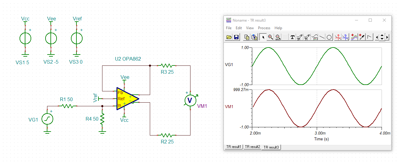
    remove R4, R12 and R13. Set R1 = R2, R7 = 0, R8 = R10 = 25R.

    What to do with R1 depends on your setup: If you drive the circuit from a 50R source, set R1 = 0. When driving from a 0R source, set R1 = R2. R1 = R2 can be set to 50R or somewhat higher.

    Kai

  • Hello Kai, We want the OPA862DEVM module to work in fully differential way. For this we have removed transformer T1 and resistor R18 and populated the link resistors R17,R19 and R20.

    In the shipped module for 1Vp-p voltage, we received the single ended output of 120mVp-p.
    Now after reconfiguration, for 1Vp-p voltage, we are getting 80mVp-p (differential output).

    We want the device to give same output as that of input, i.e., for 2Vp-p single ended input, we should get 2Vp-p differential output. For this you have suggested to remove R4, R12 and R13. Set R1 = R2, R7 = 0, R8 = R10 = 25R.

    Is this suggestions valid after reconfiguration?

    Also we have the input impedance of 1 MOhms, So R1 = R2 = 1MOhms?

    Thank you in advance.

  • Hi Harpreet,

    yes, the suggestion is still valid.

    But R1=R2=1M is a bit high, as the input bias current of A1 can be up to 3.1µA according to datasheet. I would choose R1, R2 not bigger than 1k, eventually 10k if still stable.

    Kai 

  • Hi Kai,

    As suggested by you, we have removed R4, R12 & R13. We adjusted R1=R2=51R(instead of 50R), R8=R10=25.5R(instead of 25R) and R7=0R. We obtained the following attached results, which is not providing unity gain also has an offset of 60mV-70mV in  the negative cycle on the waveform. The images of the aforementioned testing are attached. The following oscilloscope waveforms were taken with DC Coupling settings and input waveform frequency is 100 Hz.

    We desire unity gain and no offset. Kindly suggest us procedure for the same.

  • Hi Harpreet,

    should look like this:

    harpreet_opa862.TSC

    Kai