This thread has been locked.

If you have a related question, please click the "Ask a related question" button in the top right corner. The newly created question will be automatically linked to this question.

TLC072:

Part Number: TLC072
Other Parts Discussed in Thread: TLV9154, TLV9152, TLV9102

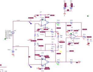
I use TLC072 to build a instrumental OP-Amp in capture CIS and do simulation in PSpice. 

As I don't have this part model in my lib, so I download this spice model-sboc020a.zip from your website.

After I complete the transfer from spice to PSpice for this model, in can simulate in PSpice.

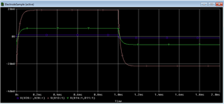
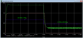
But, when I set the CM volt in my circuit as negative value (below 0Vdc, for instance is -2Vdc), the simulation result isn't symmetry with the positive value (for instance +2Vdc).

This result makes me confuse, so would you please help me to check if the part PSpice model is the c 
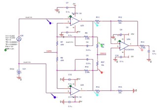
TLC072-PSpiceModel-Check-with-TI.xlsxorrect without any problems?

Attachment files are the circuit I use and simulation result I got.

  • Hello Cici, 

    Thanks for an interest in ti's products and welcome to the e2e community! 

    The legacy model was created to be used at VDD = 5V, in single supply (5V & GND) or dual supply (±2.5V). 

    In the circuit configuration attached above, there is split supply but it is ±5V, it should be ±2.5V to be compliant with the model. Please try the lower supply range to see if the model is compliant with common mode. 

    Additionally, is there a reason you have chosen a legacy device? I believe one TLV9154 will complete your design (including a reference buffer) for a lower price point! There is a PSpice model available on ti.com: https://www.ti.com/lit/zip/sbomb53

    All the best,
    Carolina

  • Thanks Caro.

    The part number we use for product (it's old product) is TLC072idg4, and the schematic is from what the older engineers created.

    Can you help to make sure TLC072idg4 has the same supply with picture you attached? That is "in single supply (5V & GND) or dual supply (±2.5V)"?

  • Hey Cici,

    Just to clarify, the device TLC072IDG4 has a max supply voltage of 16V and GND or ±8V. However, the model was developed for single supply 5V or ±2.5V. Our newer devices are modeled at the max supply range, but this is a legacy device with an old model created just for the 5V electrical characteristics table.

    Best,
    Jerry

  • Ok, I got it. Then, can I use TLV9154 which is recommended by Carolina to replace TLC072IDG4 in simulation?

  • Hey Cici,

    The TLV9154 was suggested as a replacement/upgrade in this design. TLV9154 would not function as a 1 to 1 replacement in simulation to the TLC072, these devices have different characteristics.

    TLV9154 is a more up to date part with higher performance, and requires only one device to complete the design as you have 3 op amps for your discrete INA and can use the extra op amp as your vref buffer.

    See the below comparison table, the bold number is where one part performs better than the other. Slew rate, a small voltage noise difference and a difference in short circuit current limit should not harm your design. 

    ► Part Number TLC072 TLV9154
    Manufacturer TI TI
    Channel Count 2 4
    Vs Range 4.5V to 16V 2.7V to 16V
    GBW (MHz) 10 4.5
    Slew Rate (V/µs) 16 21
    Vos max @ 25oC (mV) 1.9 0.675
    Vos Drift, typ (µV/oC) 1.2 0.35
    Rail-to-Rail No In, Out
    IQ typ (mA) 1.9 0.56
    VN (nV/√Hz) 7 10
    ISC typ (mA) 100 75
    IBias (Max) (pA) 50 ---
    Operating Temperature (°C) -40 to 125, 0 to 70 -40 to 125

    Best,
    Jerry

  • Thanks for your recommendation Jerry.

    Do you know the cost information of TLV9154?

  • Hi Jerry, my understanding is i can use TLV9154 to replace TLC072 in my circuit design, even though these two parts don't have "1 to 1 replacement in simulation".

    I tried TLV9152 simulation model that Caro provided.

    Circuit is the same with initial, only change TLC072 to TLV9152 for U26 and U27

     .

    Performance and questions with TLV9152

    1.  When set V21=0Vdc, biggest value of V1 (V28) is 0.355V, biggest value of V2 (V28) is 1.7V;
    2.      
    3. When set V21=0Vdc, value of V1 (V28) is 0.4V, value of V2 (V28) is 1.7V, there is signal fluctuation in green voltage channel, why can this happen?
    4.  
    5. When set value of V1 (V28) is 0.001V, value of V2 (V28) is -0.001V, the range of V21 is (-0.65V, 0.81V), V21 is the common mode source in my design. common mode input range should be much more wide than this in datasheet, so why can this happen?
  • Cici,

    For the question on number 3, are you doing any sort of noise modeling? Also is V1 0.4 or -0.4? You may be hitting the input limit of the model.

    For the question on number 5, your gain is 5, on the first stage, correct? When adjusting your input common mode, what does the voltage on R14 and R11 go to?

    Additionally, could you archive the project and include it here?

    How to archive:

    1. Save the .dsn file

    2. Go to file > archive project

    3. Send the .zip file (you can insert it with the insert function on E2E)

    Best,
    Jerry

  • Hey Cici, 

    Was this issue resolved? 

    I will mark Jerry's response as "TI Thinks Resolved," please let us know if you require additional help. 

    All the best,
    Carolina 

  • Hi Caro, I create a new project for this INA design- I removed other functional circuit to make the circuit and simulation result only for this INA circuit.

    Now, I have no problem which I met on Oct 13.

    But, I met other question, I will try to offer the project to Jerry for better communication and understanding.

    So I'd like to keep this issue open for advanced communication.

  • Hi Jerry,

    Sorry for reply late as I have vocation in the past weeks.

    After receiving your email, I tried to create a new design- removed other functional circuit in design, only left INA circuit. By this, I thought I will get more accurate simulation result.

    Attached design .zip is the INA design I used.

    Questions for this design is when V4=0Vdc and 2Vdc and 3Vdc and 4Vdc, simulation result is correct; but when V4=1Vdc, there is a simulation error. So why can this happen when change OPA to TLV9152?

    Please help to check this error. 

    Thanks a lot!

    ina-test-tlv915x-2021-11-02T07-07.zip

    Test-V4 is 1Vdc-Error.zip

  • Hey Cici, 

    I opened your archive project and also ran into some convergence issues. 
    These are the steps I took to remedy: 

    1. Turn on autoconverge (this is located in Simulation Settings -> Analog Simulation -> Auto Converge -> Select All) 
    2. Remove TLV243XA (even with autoconverge, the sim runs really slowly), I recommend upgrading to TLV9102. 
    3. In schematic page 2, if the V4 is 2V (greater than 1), the bottom op amp rails to the positive supply voltage. 

    I am not quite sure what is happening in the second page overall. It seems like this implementation is more sophisticated than the ones I have seen the past....why? Texas Instruments has an existing cookbook recipe for discrete bandwidth INA circuit.

    All the best,
    Carolina