This thread has been locked.

If you have a related question, please click the "Ask a related question" button in the top right corner. The newly created question will be automatically linked to this question.

VCA824: output baseline is different under different gains

Part Number: VCA824

Hi team,

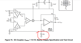
When customer is using VCA824, they found that the output baseline is different under different gains. For example, the output baseline difference between 0dB and 26dB gain is more than 100mV, even if the input and output circuits are disconnected, it is the same. Different VCA824 chips perform differently ( High and low gain baselines are different). They saw the output and input offset zeroing circuit in Figure 67 on page 23 of the data sheet. I would like to trouble you to confirm it. Is the zeroing circuit necessary to ensure that the baseline is consistent? Is there a way to ensure that the baseline is consistent.

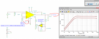
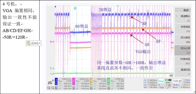
In the following picture, VGA gain are the same(-50R/+100R) but the output baselines are different(Blue/Orange/Pink are very different, nearly >100mV).

Any advice about this?

  • Morning Amelie,

    It is likely you are seeing the effect of DC error terms that do vary part to part. Have they attempted a DC error analysis from the spec range. The TINA models only have one placeholder number in them for DC errors, but there is a range.  Looking at the circuit - a few comments, 

    1. The Rf and Rg are relatively high - that increases both the noise and some of the DC error terms

    2. the GND pin - normally I would recommend putting a 20ohm to ground there to deque the emmitter followers looking into that node. 

  • Just kind of scanning through the datasheet, yes here is that 20ohm on the V+ input of the output amplifier - I put that there back in the 90's as the original version of this part (CLC520) oscillated at 1.2GHz if I didn't. May not be necessary for the VCA824, but good practice 

    At one point I thought I had put a DC correction servo loop example in these datasheets. You are AC coupled, you could add that with a correction signal into that GND pin to servo the DC output to whatever you want - essentially correcting all the part to part and over gain DC errors. It is labeled GND, but it is actually the V+ node of a CFA output amplifier. 

  • Hi Amelie, just to confirm, yes you can use the circuit in Figure 67, although it will have to be tuned for each individual device.

    As Michael says, there is another possibility that will work without specific tuning since you are using AC coupling. You can use an amplifier to integrate the VCA824 Vout against a reference, and drive the non-inverting pin of the second internal amplifier stage. This will make sure that the output average is consistent.

    Best regards,

    Sean

  • Here you go Amelie, I had some time this morning to step through this, the TINA file is the last one in here with the input C shorted

    VCA824 with servo loop testing.docx

    VCA824 with DC output servo amp.TSC

  • And here I reduced the Vg to 0V, note the output DC did not change with the servo loop amp in there, 

  • Thanks Michael!

  • You bet, of course for now (without adding the servo amp) you should reduce the Rf and Rg and will see better bandwidth on the exisiting board and just recognize the DC is going to change - you could of course also output AC couple that to remove.