This thread has been locked.

If you have a related question, please click the "Ask a related question" button in the top right corner. The newly created question will be automatically linked to this question.

I-V stage calculations

Part Number: THS4551
Other Parts Discussed in Thread: PCM1794A

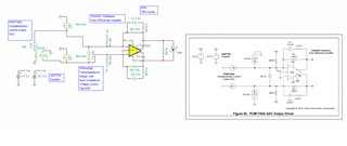
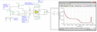
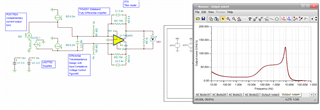
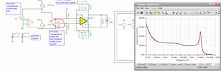
Hi, i'am looking at schematics on page 52 of ths4551 datasheet ( ths4551 as I-V stage for PCM1794a DAC) and I can not figure out how high-frequency noise gain is calculated (and the value of capacitor between differenitial inputs). Why it is 17.7 V/V?

  • Hello Vladimir, 

    This was work I was doing back in the Augf2016 timeframe and the linked file to this circuit does still work - using the original THS4551 TINA model that I worked on with Mr. Theodorus. 

    So briefly, whenever we add a feedback cap to bandlimit the signal path as done here, you are effectively dropping the noise gain to 1V/V at higher F if you don't do anything else. A lot of these FDA's are aggressively compensated to keep as high a loop gain at lower F as we can on very low supply current. Hence, since audio does not care much what is going at the FDA outputs above a certain frequency I used that differential C across the inputs to shape the noise gain way up at frequencies above the audio band to make very sure the FDA stayed stable. To see that noise gain, double the differential value to tie two of those to ground as an equivalent circuit - then the higher F noise gain set by the cap divider is 1+ 40nF/2.4nF = 17.67V/V  - kind of arbitrarily high without putting much thought into it.  

    You can easily see the effect of no input diff C by looking at the output diff noise through about 400MHz, should have a sharp peak where LG xover happens, yes, that spike indicates very low phase margin, Incidentally, this inverting noise gain shaping was something I published long ago for BurrBrown, recently republished here,

    https://www.edn.com/unique-compensation-technique-tames-high-bandwidth-voltage-feedback-op-amps-2/


    Putting the 20nF back in, and yes there is a noise gain peaking and still some resonance back around 10Mhz, but not low phase margin. The RR output stage has a lot of resonance in it also and does not like direct C feedback - hence those little 4.4ohm R's. I believe there is a model update, but seem to recall it lost that Zol resonance that is in the physical device. These issues are not unusual for low power RRO FDA's. 

  • ОК,I uderstand the point. But this method of compensation significantly degrade THD performance of the circuit due to 25db loss of loop gain and large level of output noise of 1792/94 (as any of delta-sigma DACs) at 40-400KHz range. Is there possible to increase value of this 4Ohm resistors to 20-40Ohm and make HF Noise gain lower, say 2-3 V\V?

  • Well the feedback pole is current set at 88kHz - do you want it somewhere else - and yes, this is an extreme NG peaking assuming max audio at 20kHz - if you are using the PCM DAC for something higher, the design can be tuned up I am sure - I suspect a NG shaping to 3 would be adequate for phase margin. 

  • Looks like you are done here, I did easily find some work I was doing to test the new model - you might want to use the old one we attached to the datasheet example circuits, I had done a series of 18 AudioXpress articles, this was some background work while doing those, 

    THS4551 model concerns in testing new vs old one in an MFB design.docx

  • Here I changed the diff C to equal the feedback C, that makes a noise gain of 3 at higher F, yes, we see the noise gain peaking but no sharp spike at higher F