This thread has been locked.

If you have a related question, please click the "Ask a related question" button in the top right corner. The newly created question will be automatically linked to this question.

THP210: Should a designer follow the data sheet or an EVM design for a particular device?

Part Number: THP210
Other Parts Discussed in Thread: , OPA325, THS4551, OPA320, REF5030, THS4561, OPA350, OPA365

Hi,

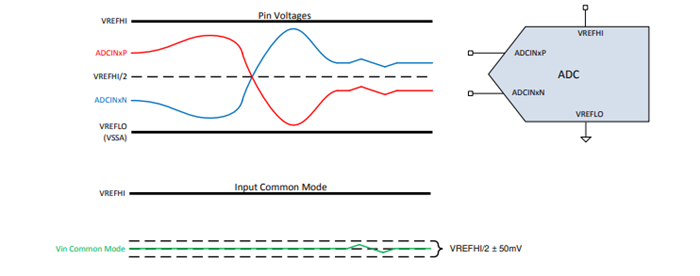
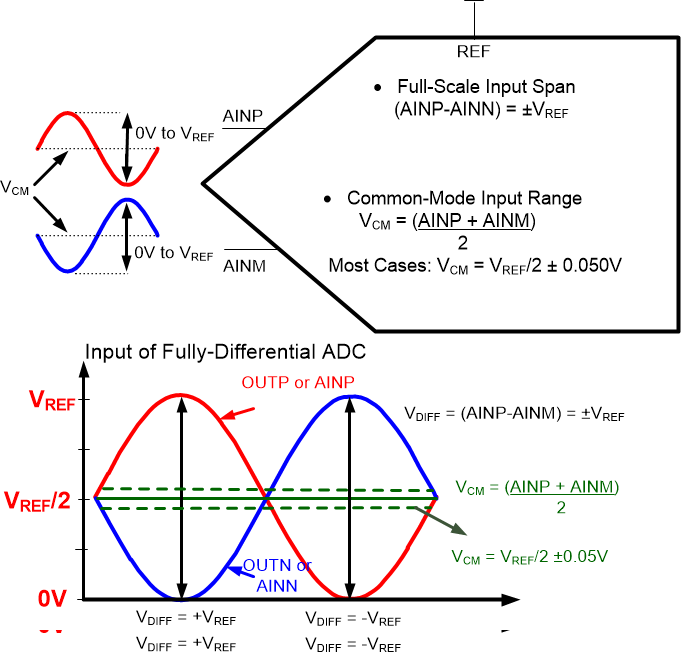
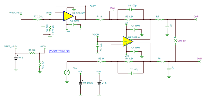
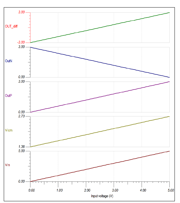
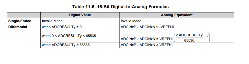
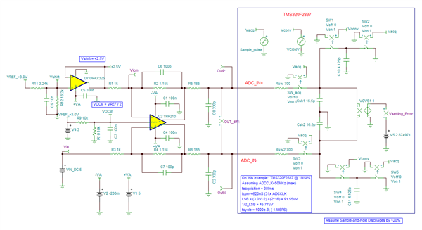
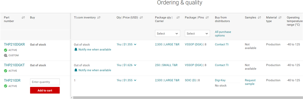
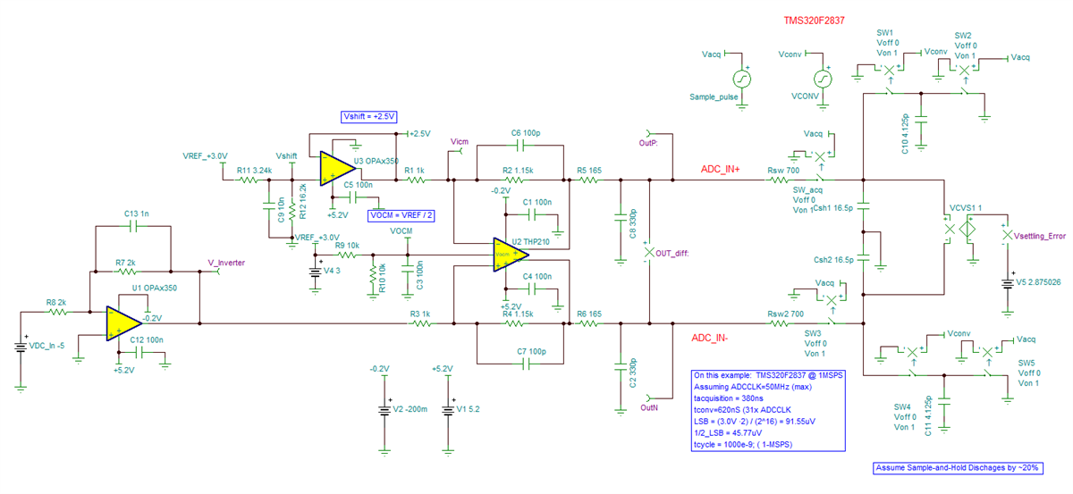
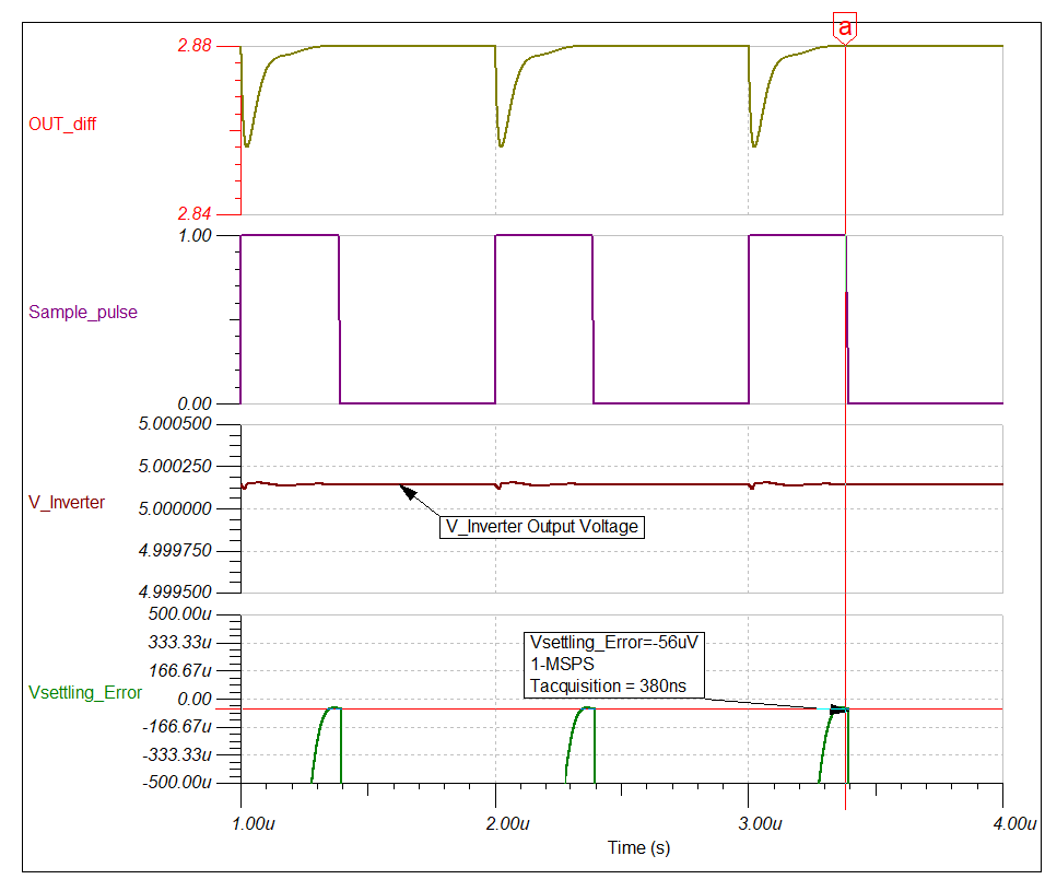
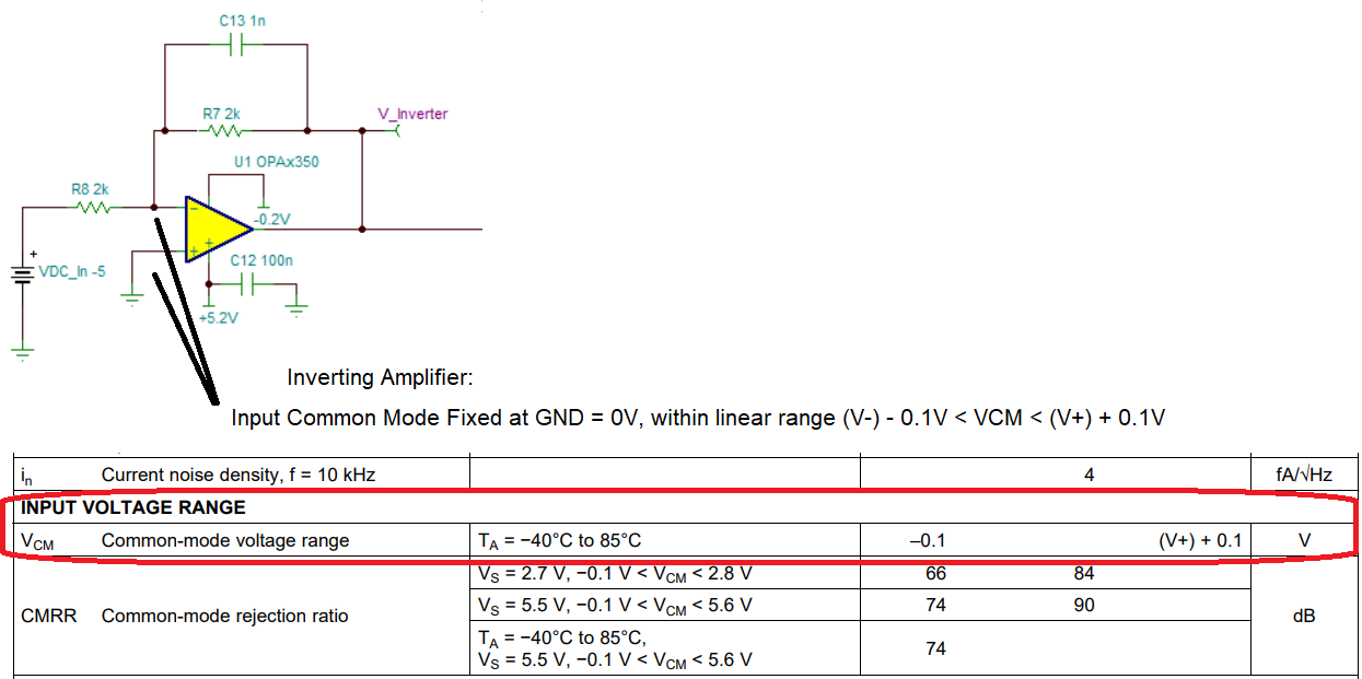
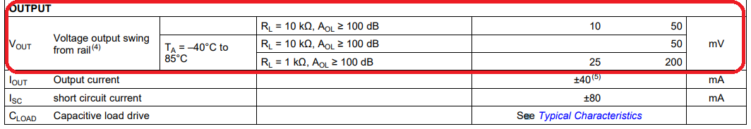
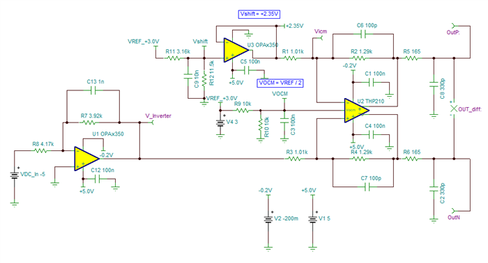
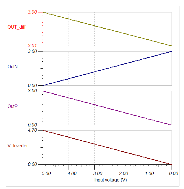
I am looking to use the THP210 to change a single-ended voltage source of 0-5V to a differential representation for measuring by a 16-bit differential ADC. 

My question is, should I use the design that is in the EVM for this particular device, or would it be better to follow the more simple designs that are included in the data sheet?

best regards,
Joel

  • An additional question, if I may: 

    If I want to use this device to convert a 0-5V ground referenced DC only signal, to a differential voltage that has maximum 0-5VDC output, is this possible? If so, would one set the common mode voltage as zero such that the full 0-5V output voltage swing can be achieved?

    Do you need a negative voltage supply if the input voltage to the THP210 does not go below 0V? Is this device OK to use for DC only signals or is it more often utilized for only AC signals?

    Joel

  • Hi Joel,

    what ADC are we talking about?

    Kai

  • HI Joel,

    The THP210EVM demonstration board has extra component footprints to allow flexibility.  This is done to facilitate the implementation of different circuit configurations and filters.  Your circuit will need to be customized per the application.

    The VOCM sets the output common-mode voltage of the Fully-Differential amplifier. In general, the VOCM voltage is set to meet the input common-mode voltage requirement of the differential input ADC. 

    Different ADC devices may have different input common-mode voltage requirements. For example, some ADCs require a input common-mode voltage that is set at the middle of the supplies while others require a common-mode voltage that is at the middle of the full-scale range or VREF / 2.  Which ADC device are you driving and what is the input common-mode voltage requirement on the ADC?  What is the ADC reference voltage and the ADC full-scale range?

    The device can be used for DC or AC signals.

    Please let me know which ADC are you driving or what is the input common-mode voltage of the ADC and reference voltage.

    Best Regards,

    Luis

  • Hi Luis, 

    I am using the F2837xD series of Digital Signal Processors. The 16-bit differential ended ones. 

    I am going to try and simulate the device in TINA but the only thing I am confused about it the VOCM chip, but that's because fully-differential amplifiers are new to me. I thought it was simply an offset at first, but not entirely sure. I have a 0-5VDC input referred to ground and I just need to convert that to 0-5VDC but differential so I can take advantage of the extra 4-bits in the differential ADCs!

    Best wishes,
    Joel

  • Hi Kai, please see my answer below. It is the ADC on the F2837xD series of DSPs. I should have made that clear, sorry.

    Joel

  • Hi Joel,

    The F2837xD 16-bit fully-differential ADCs require a common-mode voltage of VREFHI/2.  Therefore the VOCM pin of the THP210 should be set to this voltage.  These controllers are often powered with a 3.3V supply, and the reference voltage can be set to a voltage in the range between 2.4V to the supply VDDA

    We will require to adjust the gain of the THP210 to make use of the  full-scale range of the ADC and will require an R-C-R charge kickback filter between the THP210 output and the ADC input. 

    What reference voltage are you planning to use?  For example, if VREFHI=3.0V, you will set the THP210 VOCM = 1.5V. 

    I can provide you a quick simulation once you let me know the reference voltage on this application.

    Many Thanks,

    Luis

  • Hi Luis,

    Thank you so much for helping regarding this. The reference voltage on my design is REF3030AIDBZT which to my knowledge is 3V. Is the gain of the design not to be fixed at 1, such that 5V at the THP210 input is translated to 5V at its output, or is this affected by the VOCM of the device? 

    The quick simulation would be very helpful, thanks!

    Best regards,
    Joel

  • HI Joel.

    Below is a figure of the F2837xD ADC input common-mode requirement, where the THP210 VOCM pin needs to be set to VREFHI/2, in this fashion the OUTP/OUTN voltages swing positive and negative in reference to this voltage or where the output signal is fully differential around a common-mode voltage (VOCM). 

    The diagram below shows the fully-differential output of the Fully Differential Amplifier (FDA), centered around VOCM, where both OUTP and OUTN swing from close to 0V to VREF, for a fully differential range full-scale range of ±VREF.

    Thank you and Regards,

    Luis

  • HI Joel,

    Thank you, I will get back to you shortly with the simulation.

    Luis

  • Hi Luis,

    Makes complete sense, but what I do not still understand is how this above action works when one of the inputs is a ground, 0V. 

    I note that the VOCM needs to be within 50mV of the ADC reference voltage, I assume one would require a linear regulator to achieve this with accuracy better than those levels? It would not be sufficient to use a voltage divider attached to the +5V supply of the amplifier itself?

    Just a note, by the way - I say I need 0-5V because on the DSP board manufactured by my university, there is a voltage divider on the inputs to the DSP which give me a 0-3V full-scale ADC voltage when I design the differential op-amp to give 0-5V. 

    Is a 5V supply sufficient for this device? I assume it can perform rail-to-rail?

    Best regards,

    Joel

  • HI Joel,

    The full-scale differential range of the ADC is ±VREF or ±3V, or a total range of 6V.  The input signal in this application is 0-5V.  The gain required is therefore VIN/VOUT = 6V/5V = 1.2V/V.  You could choose a THP210 input resistor RIN of 1kΩ and feedback resistor of RFB=1.2kΩ.

    The THP210 offers rail-to-rail output, however as any other rail-to-rail amplifier, it can not quite reach the supply rail voltage, but only get to about ~100mV from the rail supplies.  The output swing specification varies depending on load and temperature conditions.  See output swing limitation below. 

    If the ADC has a reference voltage of 3.0V, the ADC full-scale range is ±3V, with a common-mode of 1.5V.  Each output needs to swing between +3V and GND.  The THP210 while powered with a +5V supply will easily reach +3V but can only get to about ~100mV from the negative rail (GND).  If you absolutely require to reach 0V, I suggest you use a negative supply of -200mV or more negative to keep the THP210 amplifier well inside its linear range.  (I typically use the Open-loop voltage gain (AOL) output swing specification which is more conservative to ensure the amplifier is well inside its linear region, in this case AOL specifies output swing of 200mV from the rail).   Alternatively, you could choose to scale down the THP210 gain and live with the output swing limitation.

    Regarding the VOCM pin, you can use a voltage divider on the ADC reference.  Typically using a 10k -10k voltage divider straight from the +3V ADC reference is sufficient.  Please use a bypass capacitor of 10nF or 100nF on the VOCM to limit injecting noise.

    Since the input signal is Single-Ended, 0-5V, you also need to inject a +2.5V DC signal in the negative FDA  input resistor as shown below. Keep in mind, the FDA resistor inputs are not high-impedance input so it is necessary to buffer this node for accurate results.  You will require some bandwidth for this buffer amplifier since you are driving an ADC and this node will see some charge kickback when sampling at high speeds.  The OPA325(10-MHz) is used as a buffer to drive the THP210 negative input on the example below.  You could choose using a precision 2.5V reference or use a divider from the ADC reference to generate the accurate +2.5V DC shifting signal.

    The R-C kickback filter between ADC and THP210 output would need to be tuned according to the ADC sampling rate, ADC acquisition period, and sampling capacitor requirements. This requires a different analysis.    In general, with the THP210 using 100Ω and 1nF has settled while driving other precision ADCs but this would depend on your specific timing.  In other to perform the analysis you will need to define the sampling frequency, the programmed acquisition period and conversion period in the application.

    Below is the TINA simulation files on a zip file.

    THP210_shift.zip

    Thank you and Regards,

    Luis

  • HI Joel,

    The application note below discusses using an FDA to perform single-ended to differential conversion for a unipolar signal.  Although it features the THS4551 and OPA320, many of the concepts remain the same:

    Single-ended to differential signal conversion using an op amp and FDA for unipolar signals

    https://www.ti.com/lit/an/sbaa264a/sbaa264a.pdf

    Thank you and Best Regards,

    Luis

  • Hi Luis,

    All makes complete sense. I have accepted the answer. The only issue is that the university I work for has an in-house developed DSP board that uses the F2837xD.
    This device has the voltage reference of 3V on it, and I don't think there is anywhere I can access it on the board to use it for the FDA above. Is it okay to just buy another one of these voltage references and stick it on my own developed board with the same results? It doesn't need to share the exact same reference that is used for the ADC? 

    On the board is also a voltage divider that takes the input voltage and divides it down slightly. It also has a 470pF capacitor in parallel with the lower dividing resistor, I assume for filtering or kick-back as described above. Would it be better to desolder that and use the charge kickback filter above that you outlined instead? Or is it OK to take the output of the FDA and feed that into the divider network without effecting the signal? Of course, I would then need the supplies for the FDA to be 5V and some negative voltage instead, because the divider network that is intrinsic to the board will reduce my signal level by some value... The network is 3900R, and 5600R in parallel with 470pF.

    One last question, I see that the output swings between -3 and 3V that is read by the differential ADC. Will the ADC read 0 at -3V and 65536 at 3V, which would correspond to 0V and 5V in the input signal? Do I have that wrong?

    Best regards,
    Joel

  • HI Joel,

    - As you have mentioned, the best case would be to use the same 3V reference for all circuitry, in this fashion, all the circuitry moves ratiometrically referenced to the same voltage with any drift in the circuit.  Since you are not able to access the reference, you could use a local low-drift precision voltage reference such as the  REF50xx (REF5030).  Assuming that the DSP board uses a precision reference as well, the errors will be small as long as the circuitry is referred to the same ground potential.

    - Per your description, the ADC is configured in 16-bit fully-differential configuration.  Regarding the voltage divider at the ADC inputs, does this mean that each ADC input, both positive and negative inputs (ADCAINxP and ADCAINxN) has each a voltage divider?    In general, when working with fully-differential systems, both the positive and negative paths need to be symmetrical for optimal results.  Can you provide a schematic or diagram of the DSP board showing the ADC inputs and these voltage dividers?  This will avoid confusion, I want to ensure I understand how you intend to drive the ADC.  Also if you let us know the sampling rate and the acquisition period you plan to use this will be helpful in determining the optimal RC filter to drive the SAR ADC sample-and-hold.  If you can provide this timing detail, I can look into the optimal circuit.

    - When the ADC is configured as fully-differential, it can converts the difference between AINP and AINN, where the fully-differential signal is centered around VREF/2, where both ADCAINxP and ADCAINxN swing ~0V to VREF, for a fully differential range full-scale range of ±VREF.  The analog to 16-bit digital conversion formulas are available on the TMS320F2837xD Dual-Core Delfino Microcontrollers Technical Reference Manual on p.1406 Table 11-5 (also shown below).  If you have questions specific about programming the TMS320F2837D controller and ADC, it may be best to submit a new post and consult with an expert on the microcontrollers forum; but I can help with the analog side.

     Thank you and Regards,

    Luis

  • Hi Luis, 

    Thanks again for the response. I believe that every input to the DSP has the voltage divider and capacitor combination, as below:

    Regarding the sampling rate and acquisition period, this would probably be the minimum allowed for the 16-bit conversion, since my converter is very high frequency, which causes me some issues with how fast the microcontroller can handle the ISR. So I believe from the data sheet that is 320nS. I would also use the max sampling period - I plan to switch my converter at 1MHz but I'm not sure how feasible that is with the 16-bit input. Since the data sheet for F2837xD states the total conversion time for a 16-bit signal is 915nS, I suppose that limits my sampling period to that? 

    Everything makes complete sense now regarding the conversion of the single-ended source. Thanks!

    Best regards,


    Joel

  • Hi Joel,

    Using the THP210 with the voltage divider scales the signal properly when using the THP210 on G=2-V/V with VOCM = 2.5V. However, the voltage divider is not optimal for sample-and-hold settling at fast throughputs, and this voltage divider will only work for long acquisition times or low sampling rates.

    Below is the proposed circuit.  The input signal in this application is 0-5V.  The gain required is therefore VIN/VOUT = 6V/5V = 1.2V/V.  I scale the signal slightly more to a gain of 1.150-V/V to allow some margin on the range. The THP210 input resistor RIN is 1kΩ and feedback resistor of RFB=1.150kΩ.  Use the a local REF5030 (3V precision reference) to generate the 2.5V signal at the negative input resistor of the THP210.

    The optimal R-C kickback filter per the simulation R=165Ω and C=330pF at each input.  I assumed that the sample-and-hold capacitor looses 20% of the charge between conversion to conversion.  This is a valid assumption when driving the SAR ADC on a single channel solution (not multiplexed).

    The THP210 settles to about ~1/2-LSB of 16-Bit resolution at 1-MSPS when using a 380ns acquisition period (assuming VREFHI=3V). 

    When using the minimum ADC acquisition time of 320ns with the device running at full throughput of ~1.06-MSPS, the sample-and-hold settles within ~1-LSB of 16-bit resolution. 

    I think this result is acceptable since the simulation tends to be conservative, specially if you are able to extend the acquisition to 380ns and assuming you are only continuously converting 1-single channel (ADC is not multiplexed). If you are multiplexing or converting different channels with the same SAR ADC, you will need to allow a longer acquisition time around 550ns to 600ns while using the THP210. If this is a concern, let me know, we could suggest a similar circuit tuned for a faster FDA such as the THS4551 or THS4561 that will offer faster settling.

    Attached is a pdf file with the simulation analysis explanation/summary, and a zip file with the simulation files.

    THP210_F2837xD_Settling_Analysis_L.Chioye-1MSPS_ab.pdf

    THP210_F2837xD_Settling-1MSPS_keep.zip

    Thank you and Regards,

    Luis

  • Hi Luis,

    Thank you so much for the above message. I did think the resistive divider would cause issues in the circuit so I will proceed to use the proposed circuit and desolder the resistive divider/insert an 0R resistor in series with the output of the FDA such that there is no further attenuation to the signal. I must say that the level of support you have provided is absolutely above and beyond what I expect from a forum but I am so appreciative. Have a great day and thanks again for all of the knowledge and simulations!

    Best regards,

    Joel

  • HI Joel,

    Thank you for the Kind words.  Let us know if you need anything,

    Kind Regards,

    Luis

  • Hi Luis,

    Just a couple of points regarding the circuit above if I may. It works correctly but I forgot a few things that may be issues:

    The DC voltage is actually -5V from my output. I plan to use an inverting amplifier to translate this to +5V input to the FDA. Will I need a buffer amplifier stage placed between the FDA and the inverting amplifier for the FDA to convert correctly?

    I already have a -5V feedback signal from my high voltage output going into a single-ended source 12-bit ADC. Will this also need a kickback filter? Is it OK to share this feedback voltage to another ADC, with the FDA assuming it is correctly buffered with an op-amp?

    Best wishes,
    Joel

  • additionally, what is the difference between models 

    THP210DR, THP210DGKR, and THP210DGKT? They all seem to be the same FDA with same qualities and footprints but they are available as different products. Not sure which one I should buy!

    Regards,
    Joel

  • Hello Joel,

    The THP210 is available in two packages, they both have the same pinout but the package dimensions are different.  The THP210DR is the SOIC 8-pin package, 4.90 mm x 3.91mm.  The detailed SOIC package footprint drawing (D008) is on page 39 of the THP210 datasheet.  The THP210DGK is the VSSOP 8-pin package 3.00mm x 3.00mm.  The detailed VSSOP package footprint drawing (DGK) is on page 42 of the THP210 datasheet

    In addition, the THP210DGK package is available on the large or small tape and reel.  The THP210DGKR orderable is for the large 2500 tape and reel:

    https://www.ti.com/packaging/docs/carriermaterial/carrierlookup?OPN=THP210DGKR&state=details#results

    THP210DGKT is the same VSSOP 8-package on the small 500 large tape and reel: 

    https://www.ti.com/packaging/docs/carriermaterial/carrierlookup?OPN=THP210DGKT&state=details#results

    Unfortunately, some THP210 package variants currently show out of stock.  If you want to be notified when they become available, please navigate to the THP210 product landing page under "Ordering & quality" (link below), and click on the "Notify me when available".  

    https://www.ti.com/product/THP210#order-quality

    If you have additional questions about the circuit, please provide a detailed schematic or diagram.

    Thank you and Regards,

    Luis

  • Hi Luis,

    The only thing that has changed about the circuit is that the DC input voltage is -5V, instead of +5V. Everything else is the same. I just wonder whether if I invert that with an inverting OPA, I will need an additional buffer like the one in the simulation you sent me, placed between the inverting opamp and the FDA.

    Also, the buffer in the simulation is out of stock, is the OPA https://www.mouser.co.uk/ProductDetail/Texas-Instruments/OPA365AID?qs=sGAEpiMZZMutXGli8Ay4kEvVCQFydfz%252BrcHy8EJ4V9E%3D a good replacement.

    Best regards,

    Joel

  • HI Joel,

    Yes, you are correct.  If you feed the -5V DC voltage through an op-amp in the inverting configuration, then you could feed the resulting inverting amplifier output into the FDA 1kΩ input RG resistor.   The inverting amplifier will be able to drive the FDA.  The OPA325 or OPA320 could do it.  If these op-amps are not available, you could consider the OPA350 (or OPA365 can work as well).

    Thank you and Regards,

    Luis

  • Thanks Luis,

    Would I need an additional Buffer between the inverting operational amplifier and the FDA, though? That was my concern. I know it is typical to place a buffer between OPA stages, wasn't sure if that changes with the FDA and one is not necessarily requried?

    Joel

  • Hi Joel,

    No buffer is required between the Inverting amplifier output and the FDA resistor input, as long the inverting amplifier offers relatively low output impedance over frequency (in other words, as long an amplifier with enough bandwidth is selected for the op-amp inverter).  The OPA350(40-MHz) in the inverting amplifier configuration is able to drive the FDA easily without any issues since it has plenty of bandwidth.  The OPA325 (10-MHz) in the inverting configuration (currently not available), it is still able to do it, but it has a small settling error, but still acceptable within 1-LSB.  The -5V VDC source circuit that precedes the inverter should be able to drive the 2kΩ input impedance of the inverter amplifier circuit in the example below...

    For the inverter circuit, if the signal is -5 DC and need to invert to +5V DC output, you will need to power the op-amp with a +5.2V supply (the OPA350 supports up to + 5.5V supply) to ensure the inverter op-amp output has enough headroom to the supply to drive +5V.  Alternatively, you could choose to re-adjust the gain of the inverting amplifier and FDA circuit and power the circuit with a +5V supply. 

    If this is not what you meant, please provide a schematic.

    Thank you and Regards,

    Luis 

  • Hi Luis,

    This is exactly the circuit that I meant. Thank you. The OPA350 however is able to perform as rail-to-rail, 0.3V above and below the supplies. So how come the 5.2V is required? Surely it should be able to reach 5V output for a 5V supply, no?

    I am happy to go ahead with the changing of the amplifier gain resistors instead. You have it as 1K and 1.15K so a gain of 1.15. For a 5Vin, wouldn't that only be +/- 5.75/2 of the ADC range? So not utilizing the full ADC range? If we assume that the OPA can only get 300mV from the 5V supply, so 4.7V, a gain of 1.2766 is needed, so resistors of 1K and 1.27K should do, if I am calculating correctly?

    Best,
    Joel

  • HI Joel,

    The OPA350 is rail-to-rail input and rail-to-rail output amplifier.   The OPA350 input common-mode voltage range is from (V-)-0.1V to (V+)+0.1V.  From the input perspective, on the inverting circuit configuration above, the voltage at the non-inverting terminal is fixed at 0-V; therefore the device is inside the range while powered with V+ =+5V (also for V+ = +5.2V) and V- = -0.2V.

    The OPA350 voltage output swing from rail specification is shown below, from page 6 in the datasheet.  The voltage output swing is 200mV from the rail supplies. In this application, I suggested to use at least (V+)> +5.2V to allow enough headroom for a +5V output:

    For clarification, the term "rail-to-rail output" has been widely used to define amplifiers that reach an output swing close to the rail supply, usually within a few 100millivolts.  This term has been used widely all across industry for many years.  The tutorial below discusses this topic.

    For more information about amplifier input-output range specifications, please review TI Precision Labs tutorials, Op-Amps, Section 3.  This is great material covering a wide range of operational amplifiers concepts starting with basic concepts to specific advanced topics in great detail:

    https://training.ti.com/ti-precision-labs-op-amps?context=14685

    Regarding the question on the circuit, yes, you could easily power the OPA350 and THP210 with (V-) = -0.2V and (V+) = +5V, ensuring the full-scale range of the fully-differential ADC (±3V) is covered in the circuit below. 

    I adjusted the gain of the inverting amplifier assuming -5V to +0V input for 0V to +4.7V output.  Adjusted the voltage divider for Vshift = 4.7V / 2 = +2.35V, using R11=3.16k and R12=11.5k, to inject +2.35V into the FDA inverting path, and then re-adjusted the THP210 gain to scale the signal into the ADC using the same concepts we have previously discussed, feel free to modify per your requirements.

    Thank you and Regards,

    Luis