This thread has been locked.

If you have a related question, please click the "Ask a related question" button in the top right corner. The newly created question will be automatically linked to this question.

OPA392: Accurate measurement of voltage from high impedance source

Part Number: OPA392
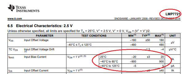
Other Parts Discussed in Thread: TINA-TI, LMP7721, LMP7715, TMUX1104, OPA387, OPA397

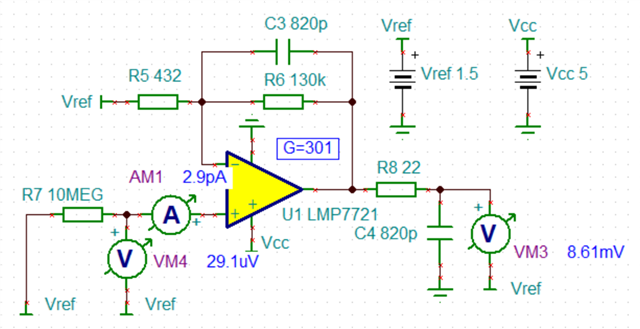
I tried to design measuring amplifier capable of amplifying (300x) high impedance (10MΩ) 0-10mV DC voltage signal.
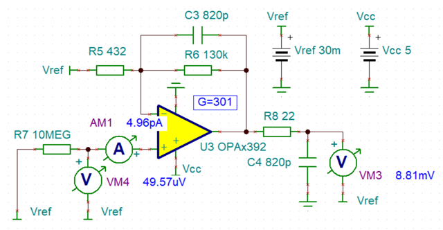
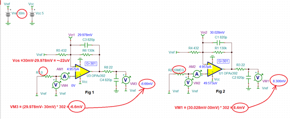
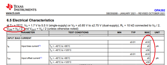
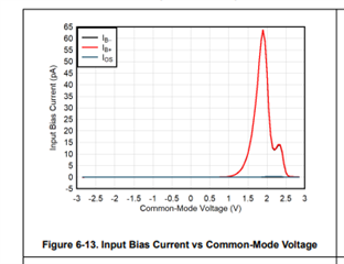
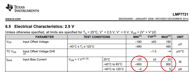
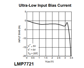
It seemed that OPA392, thanks to its super-low bias current (<<1pA) and low offset voltage (<10μV), would be a good choice for this task but even simple TINA DC analysis show high (8.8mV) output error. Error is way higher than what I expected.
How do I go about designing such amplifier?
Are there any typical/reference solutions or whitepapers on this subject available?
Most application examples show how to measure either differential or low impedance signal.

Please advise.

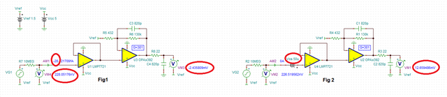
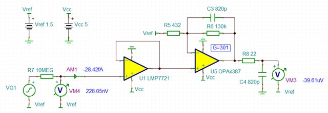
TINA screenshot and model attached.

OPA392 - test 1.TSC

  • Tomasz,

    One thing you need to be aware of is that since the output of an op amp cannot swing all the way to its rails, in a single supply operation you need to apply a small negative voltage to enable Vout to get to the system ground. OPA392 AOL specification shows 50mV to 100mV (for 2k vs 10k load, respectively) linear output swing to the rail - see below.

    Since I could not open you files, I created Tina-TI schematic, which I believe you use to gain up your input signal.  However, in order to assure a linear operation of OPA392 output stage for zero input signal, I have added 100mV negative supply Voltage - see below.

    Fig 1 shows Vos1 of -21.5uV, which after a gain of 300 correctly show Vout1 of -6.4mV.  Likewise, Fig 2 shows 49.2uV, Vin, drop across 10M input resistor (4.9pA*10M) resulting in Vos2 of 27.7uV (49.2uV-21.5uV).  Gaining it up by 300 correctly show Vout2 of 8.3mV - see below.  Thus, the output error you see is the input offset voltage gained up by 300.

    Sweeping the VG1 input from 0 to 10mV, properly shows the output voltage changing from around zero to 3V - see below.

    Tomasz OPA392 circuit.TSC

  • Hi , thank you for your response. My test design takes output swing headroom to negative supply into consideration. The signal ground is 30mV above the OpAmp negative power supply but, as you pointed out, it should probably be increased to 100mV - I was looking at the OUTPUT specs section only.

    However, what surprised me was input current much higher than expected - almost 5pA - while specs show input bias current and input offset current 0.01pA (typ). Do I misinterpret those numbers? Perhaps I do.

    Links to images and TINA file I attached take about 15s to load but eventually they show up.

  • Hi,

    here is Thomasz's simu file:

    tomasz_opa392.TSC

    Kai

  • , thanks! I have updated my initial post once I figured out files could be simply dragged and dropped.

  • Thanks, Kai. 

    Tomasz, in order to attach the files, you should use INSERT bottom shown below the Reply window.

    Other than too close operation of the output from its rail (30mV instead of 100mV), your circuit works as it should - see below.

    As far as IB specification goes, you need to look at the maximum and not typical values - see below.

    Please be aware that the IB limits are specified at mid-supply (Vcm = Vs/2).  If you change the input common-mode closer to positive supply IB+ may be much higher - see below.

    Any error due to IB may be easily calibrated out; otherwise,  you may consider using LMP7721 - see below.

  • Dzięki Marek! That makes a lot of sense. Indeed, increasing Vref to 2.5V causes Vout drop from 7 to 0.3mV.
    OPA392 may not be the best choice for this job. I did not realize IB stays low only within rather narrow range of common voltage.
    LMP7721 appears to be far better choice, LMP7715 being second choice.
    I start to think that I need two-stage amplifier. First stage with low IB/IOS and low gain, second with low VOS and high gain. LMP7721 has significantly higher VOS, which I do not want to get amplified.
    What do you think? How would you approach such challenge?

    I did not mention that gain needs to be programmable, at least 4 ranges, TMUX1104 seems to a good choice thanks to its low leakage but any additional elements in such sensitive circuit will pick up lots of EMI/RFI. This is another reason why I think two-stage architecture may be a better choice.

  • Update: LMP7721 TINA simple simulation does not yield great results either (IB=2.9pA @ VCM=1.5V). This IB is an order of magnitude higher than what I was hoping to obtain. What am I missing?

    LMP7721 - test 1.TSC

  • Tomasz,

    You may not rely on the LMP7721 macromodel to show correctly IB at fA range - instead you need to look at the specifications below. 

    IB stays flat at few fA for as long as Vcm <(V+)-2V - see below.  This means that despite what the simulation shows under the conditions shown above, IB should stay below +/-20fA at 25C.

    Having said that, any increase in ambient or junction temperature will increase IB.  For this reason, the way to make this work is to calibrate the system - this means you need to measure the output voltage for 0mV input signal and then account for it while measuring any other DC input voltage from 0 to 10mV.

  • Marek, what I am trying to accomplish is a design which does not need such calibration and is still precise enough. Precise enough in my case means 0.1%. Such precision would be more than satisfactory and I still hope this is achievable. It does not need to keep params within wide temp range.

    I will give LMP7721 a shot. I think TI should consider updating the model since it is highly inaccurate with respect to the most prominent feature of this product.
    Do you think two stage architecture makes sense in this case? The down side of LMP7721 is its relatively high VOS I do not want to get amplified.

  • Absolute precision of 0.1% on 10mv full scale input voltage range would mean that the entire input voltage error, Vos + IB*10M, need to be below 10uV.  Even though LMP7721 extremely low IB should not contribute much to the input error, its maximum Vos is much too high to get the required precision.  We have chopper amplifiers with required input offset voltage, Vos, of few uV BUT the choppers' IB is higher than 1pA needed. Using LMP7721 as a buffer will greatly diminish the IB*R error but I do not see how you can avoid gaining up its offset even if it is done in the second gain stage. Thus, I am sorry to tell you that I do not believe you can achieve 0.1% precision of 10mV input with 10M series input resistor without the initial calibration UNLESS you could find a sensor with 10x higher voltage range (>100mV) or 10x lower series input resistor (<1M).

  • Accurate model would help a lot to play around. Thank you for the help and clarification.

  • I have modified LMP7721 model to reflect IB of 28fA  BUT as you may see below this only helps if the offset is close to zero - see Fig 1.  Adding typical 50uV offset to LMP7721 results in the output error of 12mV whereas in order to stay within 0.1% initial accuracy it would have to be lower than 3mV - see Fig 2.

    I have attached the latest schematic for your convenience.

    Tomasz_LMP7721-OPA392.TSC

  • I may be able to use 5MΩ signal source and accuracy >0.25% may be acceptable so I think this design has some chance to fly.
    I may also use OPA387 instead OPA392. It has much lower VOS within the entire VCM range. See screenshot below.
    Again, thanks a lot!

  • One more comment to those who may come across this thread.
    What I initially failed to notice was that, according to docs, OPA392 maintains low IB (-20/+30fA) within VCM=±1.5V range (is it relative to VS/2 ?) and above VCM=1V IB+ goes through the roof. The available TINA-TI models for both OPA392 and its sibling OPA397 do not seem to reflect it correctly. This is probably a topic for another thread.

  • OPA392 maintains the ultra low IB (in the range of tens of fA) for the input common-mode voltage, Vcm, between:  (V-) < Vcm < (V+)-2V. 

    This means for a single 5V supply Vcm must be from 0 to 3V while for dual supply, +/-2.5V, Vcm must be from -2.5V to +0.5V. 

  • So maybe OPA392 in my two-stage design could be used as a buffer as well? Its Iis not as low as LMP7721's but it may be low enough. Note that increased, non-linear IB zone (circled in orange) is present at lower VCM end as well. To avoid this range I should probably set Vref at 200-300mV (rather than 20-30mV specified in characteristics OUTPUT section) to keep IB low and linear. Too bad specs contain no such diagram for Vs=5V, only for 1.7 and 3.3V while to be effectively used with a standard 2.5-3V ADC in such scenario those OpAmps should be powered from 5V.

  • Tomasz,

    I previously showed OPA392 graph of IB vs Vcm for Vs=5.5 (see Fig 6-13 below), which shows a large IB hump (>60pA) for higher supply voltage but not for Vs of 3.3V.  For lower supply voltage, there is no large (>30fA) "increased, non-linear IB zone (circled in orange) present at lower VCM" UNTIL Vcm is above or below supplies (+/-1.65V) - this makes a perfect sense since at this point ESD protection diodes get forward-biased.  Perhaps you could use OPA392 for your solution for as long as you use a lower supply voltage (Vs=<3.3V).

  • Now I got it. I do not why I could not see it before. Thank you for your patience.
    Is it safe to assume that IB+ bump starts at VCM=3.75V regardless of VS? That means, as long as VS (and VCM) stay below 3.75V, IB+, bump does not show up at all. It may be important to know the general rule because I am going to use standard VS=5V, not 5.5V.

  • Tomasz,

    Based on the above graphs of OPA392 IB vs Vcm, it is safe to assume that there is no large IB+ bump below VCM <(V+)-2V regardless of Vs. Thus, in order to avoid the bump for Vs=5V single supply, the input common-mode voltage must be: VCM < 3V.  Also, there is no  IB+ bump across entire Vcm if Vs<3.3V

  • Proper interpretation of Figure 6-13 is critical in my scenario - VCM may change in 0-3.0V range. Thank you for the confirmation, it seems I should be fine.

  • You're welcome. Good luck. Powodzenia!