Other Parts Discussed in Thread: BUF802,
Hello,
A few things to mention regarding the BUF802 eval board, and another regarding the BUF802 chip itself.
- Count me as another end user who thought the this evaluation board came populated. I ordered the eval boards and BUF802 devices while still in "preview" status - that is when the actual chip part number was XBUF802IRGTR rather than BUF802 etc. Maybe things changed between then and the actual delivery. Having said that... $150 for a bare board?
- I now need to actually populate my bare boards, and other than the schematic pages in the BUF802RGTEVM User Guide I find no Bill Of Materials. Of course, I can fake it based on the values listed in the schematic, but it would be nice if either the schematic had more detail of the actual parts used in the design, or - preferably - a full on Bill of Materials was included in the user guide. I see a variety of footprints in the layout and I believe some are low ESL/ESR capacitors. I assume that it might be important to stick in an appropriate part there rather than some run of the mill decoupling cap I have lying around the lab.
- The schematic and layout images in the user guide pages have the appearance of being from Altium (though I am not certain). My point is that perhaps the Schematic generated once had "hover your mouse over the symbol" embedded data for all those schematic symbols the way Altium does when it outputs a PDF, but that information either was never included or has been stripped out by the time those pages made it into the User Guide.
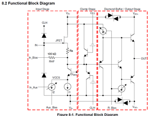
As for the chip itself question: There are a few places in the BUF802 datasheet where, based on the diagram(s), one might surmise the drain of the input FET is going to a package lead and nothing else. Elsewhere (see below) the Drain is connected to various other points in the circuit. For clarification purposes; Is the Drain of the input FET available in any way that is independent of the internal V+ "bus"?