This thread has been locked.

If you have a related question, please click the "Ask a related question" button in the top right corner. The newly created question will be automatically linked to this question.

OPA4187: Offset voltage issue

Part Number: OPA4187
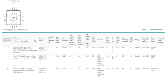
Other Parts Discussed in Thread: TINA-TI, OPA187, CC2640R2F, LM7705, OPA320, OPA2320

Hello, 
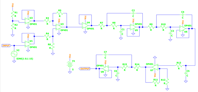
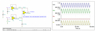
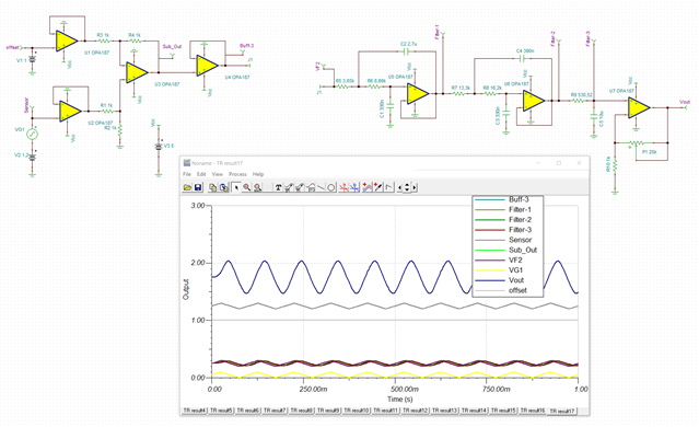
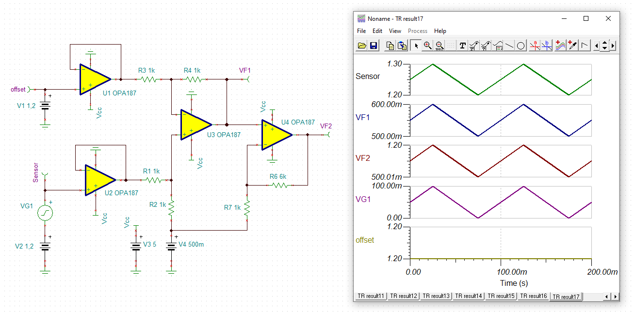
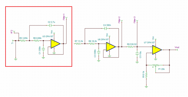
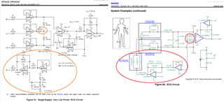
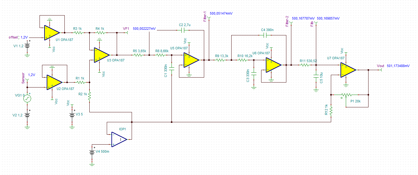
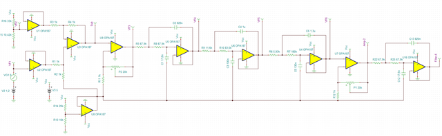
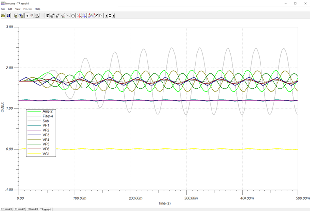
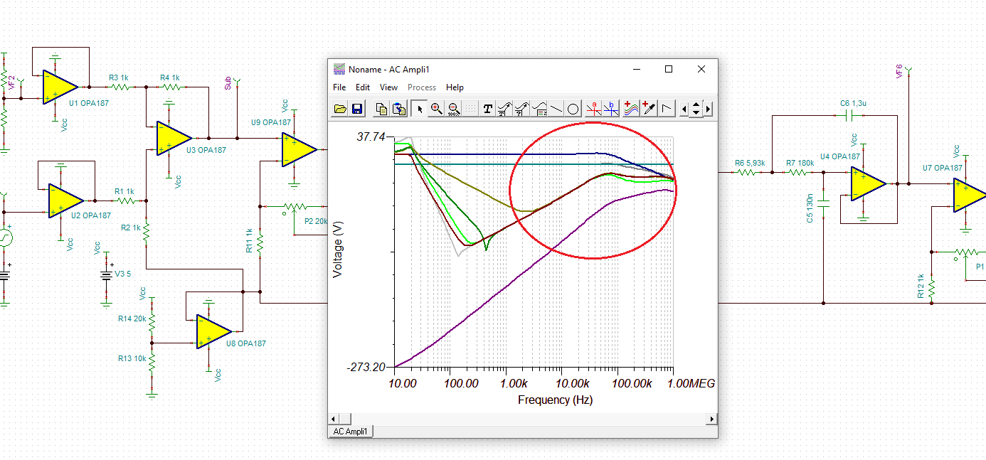
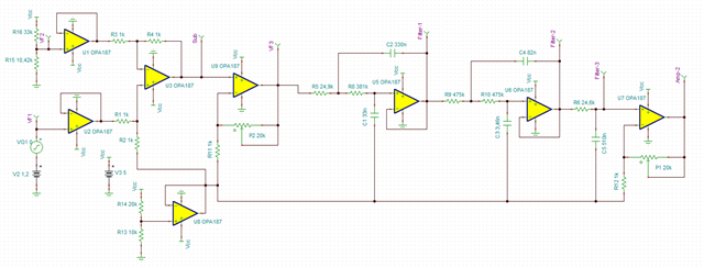
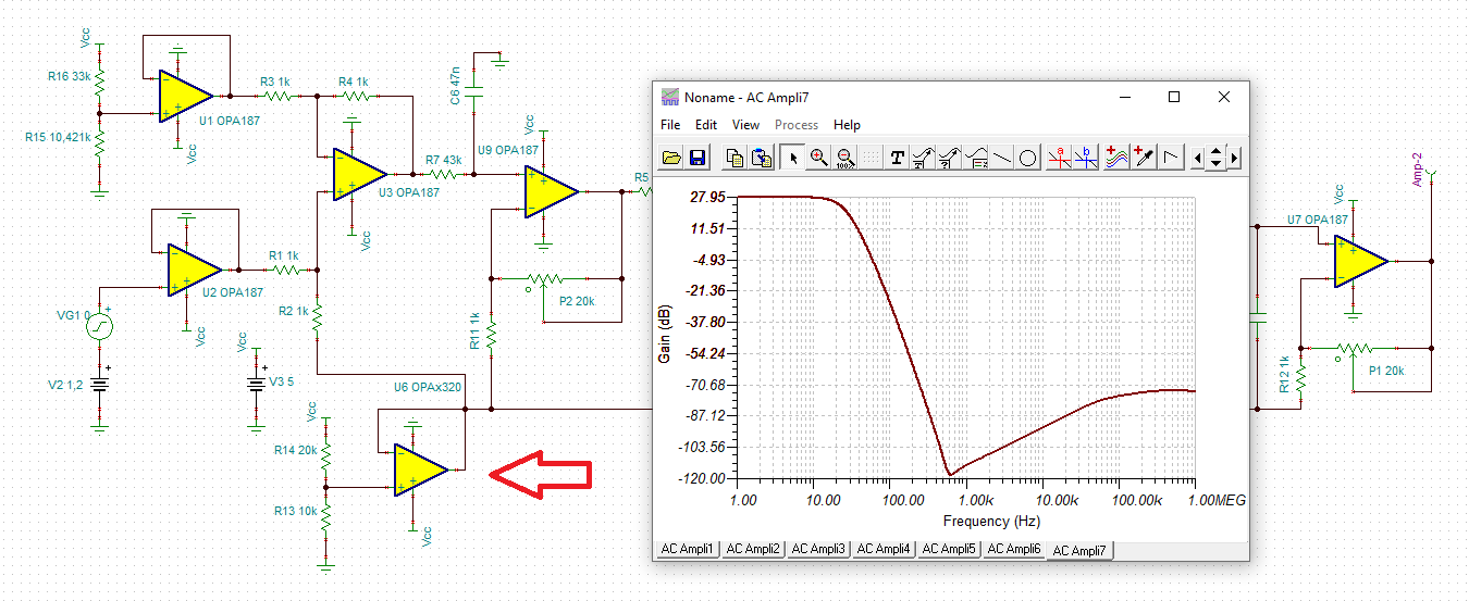
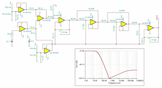
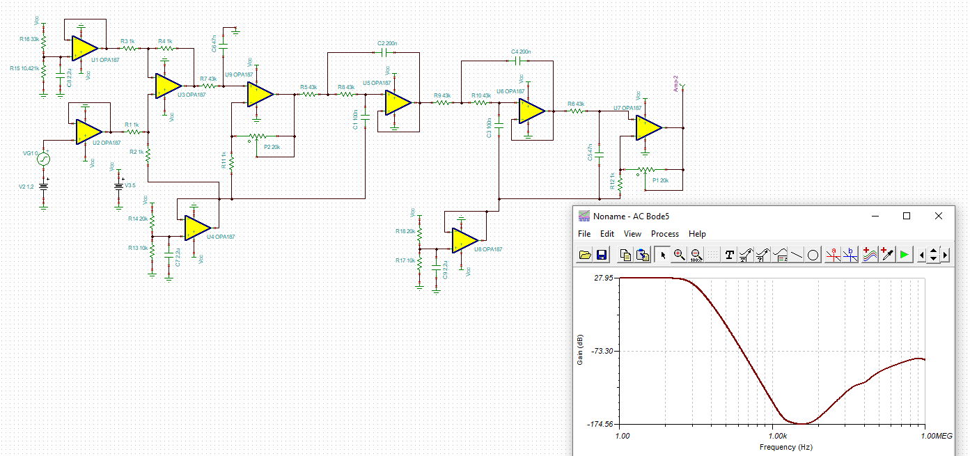
I am working on a project where I made the first prototype on a breadboard and soldered the OPA4187 opamp dead bug style on a breakout board. In the circuit, I am using two of those OpAmps. The first one is used to design three Buffer circuits and one subtractor circuit. And the second OpAmp is used to design three filters and one amplifier. The breadboard design worked perfectly. But when I designed the PCB board the second OpAmp circuit is behaving a bit odd. It has a couple of volts of offset voltage on the output of one of the filters (U5). Even if I ground the input of that filter, the output of the filter stays at around the 2-volt level. The only difference between the breadboard circuit and the PCB design is that in the breadboard design, I did not connect the thermal pad to GND and in the PCB the thermal pad is connected to GND. It's a single-rail operation.

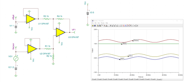
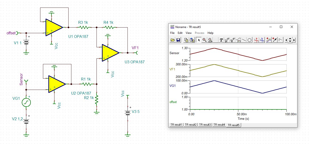
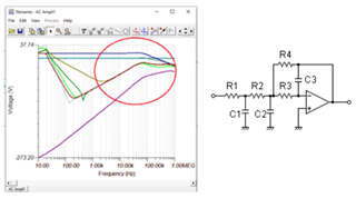
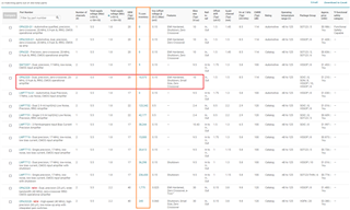
My sensor (V2) has a DC offset of around 1V that's why I am using the subtractor circuit (U3) to minimize the offset. The filters (U5, U6) are there to remove the noise, and at the end, the Amp (U7) is used to increase the gain of the signal. And the last filter (U8) is still not in use (not connected to the circuit), I may use it later on, Currently, The plan is to directly feed the Amplifier's output to the ADC pin of the MCU.

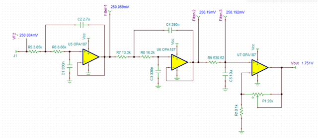
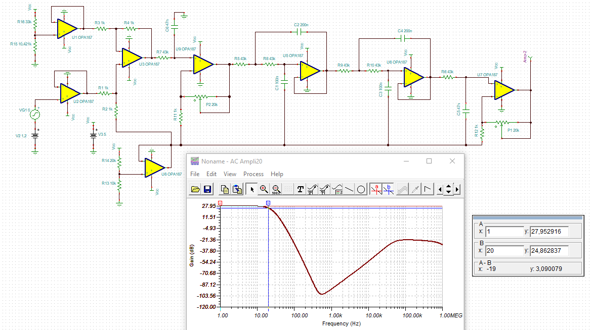
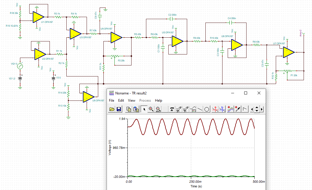
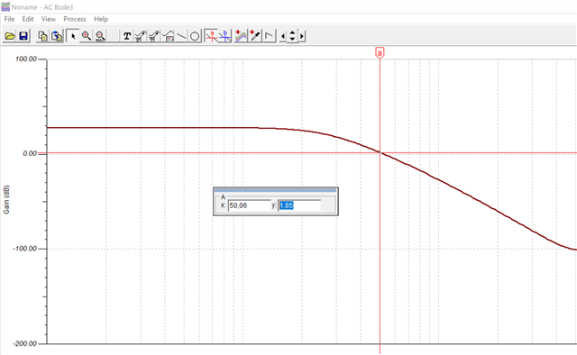
Due to having the extra offset, I am unable to use the Amplifier (U7) as it's unable to amplify the signal. When I increase the value of the pot (R11) it only increases the gain of the noise. 

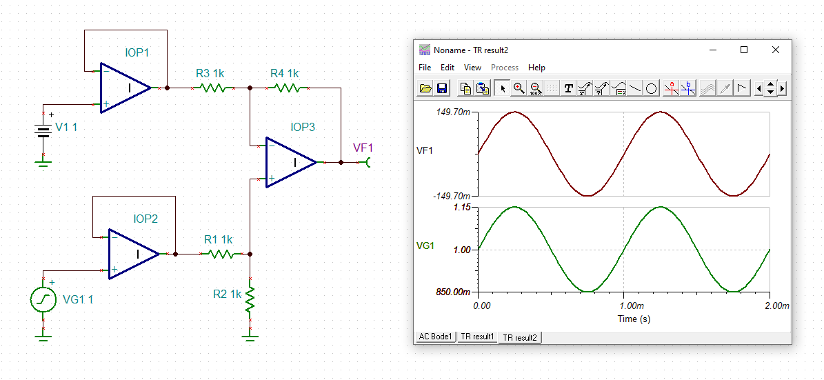
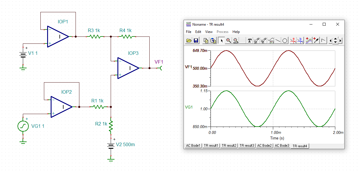
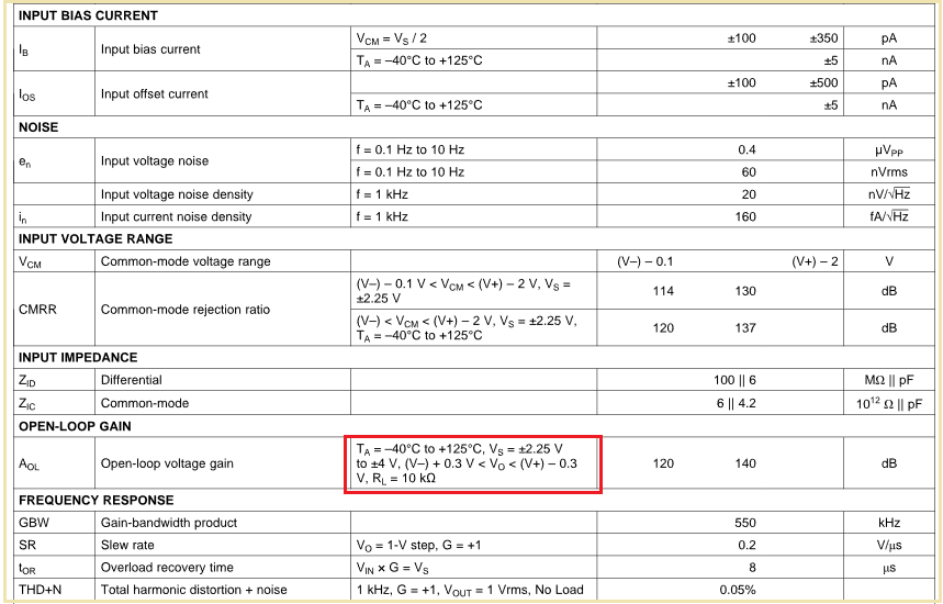
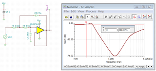
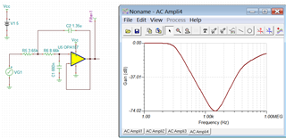
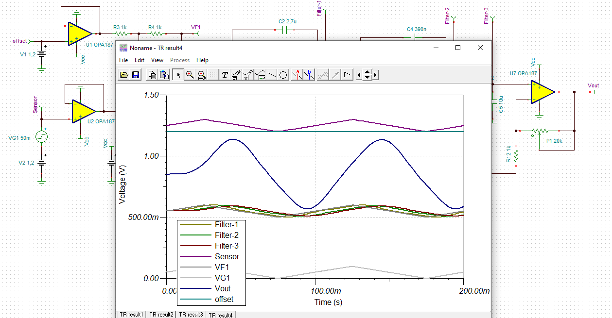
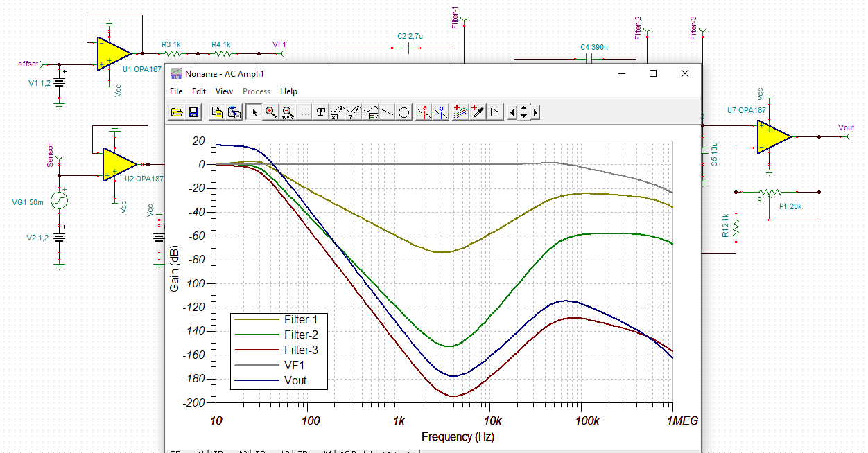
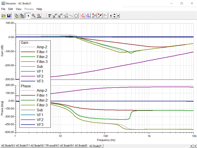
I have changed the opamp, tested each stage of the circuit separately. It looks like I am getting that offset voltage at the first filter stage. Currently, the Buffer section (U4) has an offset value of 1V (to get proper output). But the filter should not have any gain. Any idea why I am getting a higher offset value at the output of the filter (U5)?

Thank you.

  • Hi,

    there's a mistake in your circuit. The output of U3 would go into negative saturation:

    ift_opa4187.TSC

    Kai

  • Hello,

    Thank you for your reply. Can you please explain a bit more in detail? Also can you please share the name of the simulating software? I'll try to use the same simulation platform to make it relevant.

    Edited: I am using a potentiometer with U2. If the U1 has an offset voltage of 1V. I'll try to make the voltage of the voltage divider circuit of U2, as close as possible to U1. For example 0.9V. So the subtraction would be (Vu1 -Vu2)x gain = (1-0.9) V =(0.1xgain) V. SO the output voltage of U3 would be positive. That's how I thought the circuit will behave.

  • Hi,

    the simulation software is the free TINA-TI:

    www.ti.com/.../TINA-TI

    Kai

  • Hi Lfthekhar,

    As Kai pointed out, you have a difference amplifier in the first stage, see the image below. Since you are using single supply rail, your output can not go below ground. If the first stage's output is below ground, the rest of circuit is not going to work. 

    In your latest example, I simulated below. You only calculate one point. The output is the difference amplifier, then it will go below ground as shown in the simulation below.

    However, if you insert Vref > 100mV, then it will work. 

    IA_opa4187 03282022.TSC

    Regarding to the simulation tool, you may download it from TI site as shown below. 

    https://www.ti.com/tool/TINA-TI

    If you have additional questions, please let us know.

    Best,

    Raymond

  • Hi,

    Raymond was faster than me Relaxed

    Even if you set the reference voltage at U2 at the same potential as the 1V DC voltage from your sensor, the output signal of U3 would go into negative saturation with a true AC input signal:

    This behaviour can often be seen in single supplied OPAmp circuits. One remedy is to create a pseudo ground, for instance at 0.5V as shown here. (It's not 100mV as shown by Raymond, because I thought that the amplitude of your input signal is 150mV):

    The idea of the pseudo ground is to allow the OPAmp to fully swing in its linear range without going into saturation at the inputs and the output.

    Usually, pseudo ground is set to midd-supply. But with the OPA4187 you must keep in mind that the common mode input voltage range is limited to 2V below the positive supply voltage. See the datasheet. So, pseudo ground should be set to a smaller potential than midd-supply here.

    Kai

  • thank you for your reply. I think I have understood your explanation. To me it seems like my model of the sensor is a bit more different but I might be wrong.

    In my design, the U2 is connected to the sensor, and the U1 is connected to a voltage divider circuit which is adding the offset minimizing voltage, here I am modeling the voltage divider circuit with only one DC source (V1). I have created a simulation in TI-TINA. Here my sensor can be modeled as a combination of "VG1" and "V2" because my sensor has always a DC offset voltage. It's a pressure sensor. So when I don't exert any force on it, it stays at 1.2V level (offset) and when I press on it, depending on the amount of force it may go till 1.3V, and again when I stop exerting force on it, the voltage level goes back to 1.2V. So the sensor value never goes below 1.2V.

    Please correct me if I'm wrong but it looks like I should not have the saturation issue in my design.

    Best wishes,
    Ifthekhar

    Subtractor.TSC

  • Hi Ifthekhar,

    congrats for succeeding with TINA-TI Relaxed

    I read the label in your simulation "sine (1 0.1 15)" as 1VDC superimposed by a 15Hz sine wave with an amplitude of 0.1V.

    To simulate an unipolar signal instead of a bipolar signal you can use a triangle wave:

    ift_opa4187_1.TSC

    Keep in mind, though, that for linear operation the output voltage of OPA4187 would need to stay at least 0.3V away from the supply rails:

    In your circuit it is only 200mV so far.

    Kai

  • Hello Kai,
    Thank you, I'll keep that in mind Relaxed.

    Keep in mind, though, that for linear operation the output voltage of OPA4187 would need to stay at least 0.3V away from the supply rails:

    As we now know the first part of the system is working. I have added the rest of the circuit in your simulation. So, in simulatiom the Outut of the first, second and third filters (Filter-1, Filter-2, Filter-3) are were they supposed to be. But in my circuit the First filter's output has an offset value of 2V. I am not sure why I am getting that offset in my circuit.

    Best Wishes,
    Ifthekhar

    6813.ift_opa4187_1.TSC

  • Hi Ifthekhar,

    In the last stage of the circuit, the input DC bias at Filter-3 is 250mV. The gain stage of U7 or last stage is 7V/V, therefore, the output signal is centered at 1.75Vdc.

    What are the output requirements? Please let us know. 

    Best,

    Raymond

  • Hi Raymond,

    The simulation does not have any issues. It's working properly but my actual circuit on the PCB board has the issue. I am getting around 2V offset at the output of the Filter-1. Not sure why. I added a jumper in between each stage. So I removed the jumper from the input and output of the Filter-1 then connected the input of the Filter-1 to GND but still, the output of the Filter-1 has a DC offset voltage of 2V. That's the issue. I have checked the value of each resistor and capacitor in the PCB board they have the correct value, I have reflowed the OpAmp IC / changed it as well, have checked for solder bridge, short to VDD, and other signals but could not find any issue, still getting the offset value at the output of the filter-1. Not at the output of the Amplifier. Do you have any guesses, as to why it might be happening?

    Best Wishes,
    Ifthekhar

  • Hi Ifthekhar,

    no, no, Raymond is right. When you must not go deeper than 0.3V at the output of the differential amplifier (in order to keep the output stage of this OPAmp in linear operation !) and you have to amplify later, you will also amplify this offset. 0.3V x 7 = 2.1V.

    This is the moment, when you should use the trick with the pseudo ground, here 500mV:

    ift_opa4187_2.TSC

    See how I reference the gain setting resistors of the last OPAmp: The offset (pseudo ground potential) at the output of differential amplifier isn't amplified, but only the difference to the pseudo ground potential.

    Kai

  • Hi Kai,

    Thanks for this nifty idea. In my next design, I'll try to implement that, or I might cut some traces in my current board and add a voltage reference of 500mV there Relaxed

    But that was not the main issue. My first filter stage is behaving weirdly. I have isolated the first filter stage from the rest of the circuit on my PCB board. It was quite easy as I have placed jumpers in between all the stages. So right now the input of that filter is connected to GND (image shown below) and if I connect the oscilloscope to the output of that filter it shows a 2V offset voltage. I am not sure why that is happening. 

  • Hi Ifthekhar,

    The Sallen-key filter should behave like as an op amp buffer, where the output should follow the input at DC.  You have mentioned that you have checked all the component values. I can not think of a reason that the output will have 2Vdc when input is grounded (unless there is a mistake somewhere). Have you considered to replace OPA187 as an alternative?  

    The only thing I have is the following, but it is occurred at AC. 

    From the simulation, there is Q near your frequency of interest. And you need to deQue the gain peaking for Sallen-Key filter. The easiest way is to increase C1 and reduced C2. 

    So I doubled C1 value and reduced C2 value by half and it will not affect the filter's cutoff frequency. But this is not related to your 2Voffset issues. 

    OPA187 Sallenkey filter 03302022.TSC

    Please let me know what you find. 

    Best,

    Raymond

  • Hi Raymond,
    Again thanks for your reply. I have reflowed the OpAmp when the reflow process did not work, I soldered a new OpAmp but still the same issue. Also have changed the values of the capacitors as you mentioned. The weird part is that when I built the circuit on the breadboard, it worked properly. 

    I will try to rebuild the breadboard circuit. And will go with a little bit different design. You and  both have mentioned a few improvements that I can make in the design. I'll include them as well. Do you and  have any other suggestions that I can introduce to this analog circuit that can make it more robust?

    Just a short note on the design, the sensor data has an offset of 1V when no force is applied to it and when the force is applied, the amplitude goes as high as 30mV more, so the range is 1.00V to 1.030V. The signal from the sensor is associated with high-frequency noise and I want to remove the 50Hz noise as well. That's why I went with 0 to 20 Hz bandwidth for the signal and the 5th order low pass filter. The subtractor circuit is there to remove the offset so that in the later stage, I can use the full range of the amplifier. In the end, the amplified signal will be fed to a microcontroller (ADC). the Microcontroller is running on 3.3V and the ADC reference is also 3.3V. The idea was to use the subtractor to minimize the offset as much as possible to amplify the signal as much as I can without exceeding the 3.3V level. I am using the CC2640R2F BLE-enabled MCU. Also, do you guys think that I should change the Opamp? I am trying to develop a battery-powered low power consuming wearable device. 

    Thanks again for all the helpful suggestions.

    Best wishes,
    Ifthekhar

  • Hi Ifthekhar,

    So right now the input of that filter is connected to GND (image shown below) and if I connect the oscilloscope to the output of that filter it shows a 2V offset voltage. I am not sure why that is happening.

    I repeat myself:

    "Keep in mind, though, that for linear operation the output voltage of OPA4187 would need to stay at least 0.3V away from the supply rails."

    So, if you force the input to 0V the output would need to emit 0V as well, which the OPAmp cannot. You even not only violate this above mentioned 0.3V limit, but you also drive the output of OPA187 into hard stauration. This can be deadly with a chopper OPAmp like the OPA187. If a chopper OPAmp cannot close the feedback loop and keep both inputs exactly at the same potential, the OPAmp can totally run ill.

    So please use this 0.5V pseudo ground. And don't allow the output voltage of OPAmp to come the supply voltages closer than 0.3V!

    Kai

  • Hi Ifthekhar,

    The weird part is that when I built the circuit on the breadboard, it worked properly. 

    I am unable to account for 2Vdc offset at Filter-1 node. What has changed between PCB circuit and breadboard circuit? If you still have the breadboard, please measure the input and output voltage nodes and compare various nodes between two boards.

    Below is another technique to remove 50Hz common mode noise in a sensing system. Generally, it is difficult to build an instrumentation amplifier with high CMRR characteristics in discrete components. I do not mean to deviate what you are doing, but you should figure out what is going on with the existing PCB circuit. 

    The schematics below are found in INA826 and INA333 's datasheet.  Of course, TI has many different types of instrumentation amplifiers for measuring differential input application.  The EKG technique is to sample 50Hz CMRR noise actively, inverted its amplitude, gain it up and feed it at the sensor's input as Vcm signal.  

    I do not want to speculate which technique will work better - the above method vs. applying 5th order LPF filter to attenuate the 50Hz common mode noise. Due to close frequency range of 10Hz and 50Hz, the effect of attenuate the common mode noise may be limited. You should check it out with the simulation. 

    Please let us know what you find. Kai's suggestion makes a lot of sense, but I am unable to visualize that it will have such large offset at the output of instrumentation amplifier, even I am taking into account of large tolerances of feedback resistors (assumed the IA and LPF circuits are operating in a linear region). 

    Best,

    Raymond  

  • Hi Kai,

    Thanks for your reply. I have understood the issue but in the current PCB design, I am unable to make the changes because I have designed a closely packed board with 0201 components, and scratching/disconnecting the traces are turning out to be impossible. Right now I am about to rebuild the circuit on the breadboard with the 0.5V pseudo ground.

    1. Is it necessary to add a similar pseudo ground for the Filters as well? If it is necessary then what would be the procedure because here I am using sallen key filter and the opAmp are mostly voltage followers.

    2. Can you recommend a different opAmp that will allow me to perform the single rail operation without the need for a pseudo ground? Then I can just solder the new quad opamp on the same PCB board.

    3. I have repeated the experiment of the filter with 500mV input voltage. At the output of the filter, I  am still getting the 2V offset. the only difference between the breadboard circuit and the PCB board circuit is that in the breadboard design the thermal pad was floating and in the PCB, it's connected to GND.

    Best wishes,
    Ifthekhar

  • Hi Raymond,
    Sadly I need to rebuild the breadboard circuit. The only difference between the breadboard circuit and the PCB board circuit is that in the breadboard design, the thermal pads were floating and in the PCB, it's connected to GND. I'll rebuild it and will share the results with you guys soon.

    Thanks again.

    Ifthekhar

  • Hi Ifthekhar,

    1. Is it necessary to add a similar pseudo ground for the Filters as well? If it is necessary then what would be the procedure because here I am using sallen key filter and the opAmp are mostly voltage followers.

    Yes, adding the pseudo ground to your circuit could be done this way:

    ift_opa4187_3.TSC

    You can modify the 500mV pseudo ground potential to your needs, of course. If you are absolutely sure that the output voltage of OPAmps is never going below 500mV, then you can decrease the pseudo ground to 350...400mV with the OPA4187. But keep in mind that sensors come with offset errors which can make your input voltage going negative. Also think about eventual negative going sensor output voltages when the sensor gets a fast step and the output signal is ringing.

    Kai

  • 2. Can you recommend a different opAmp that will allow me to perform the single rail operation without the need for a pseudo ground? Then I can just solder the new quad opamp on the same PCB board.

    You will always need a certain headroom for the output voltage because no OPAmp can fully go down to 0V at the output while at the same time staying in the linear operating range. But there are many OPAmps which don't need the full 0.3V headroom the OPA4187 needs. Raymond may want to choose a suited OPAmp for you.

    A remedy which doesn't need a pseudo ground is the use of LM7705 which generates a small negative supply voltage of -0.23V. It was designed for just your application. Look into the datasheet of LM7705 to see how it works.

    3. I have repeated the experiment of the filter with 500mV input voltage. At the output of the filter, I  am still getting the 2V offset. the only difference between the breadboard circuit and the PCB board circuit is that in the breadboard design the thermal pad was floating and in the PCB, it's connected to GND.

    Are you sure everything is wired properly? No unwanted short circuit by tin solder beads?

    Sadly I need to rebuild the breadboard circuit.

    This is absolutely normal for the developping phase. Every professional designer is making modfications in the developping phase and the final boards never looks like the developping board Relaxed

    Kai

  • Hi Ifthekhar,

    My speculation is that you selected WQFN op amp package in your existing PCB layout, which WQFN is not wide available package in op amp in TI's catalog. Therefore, the selection or P2P replacement is very limited. 
    When I performed QFN package search in our database, these are the only ones that come up. Please let me know that the types of Op Amp packages you need in your exiting PCB. 

    https://www.ti.com/amplifier-circuit/op-amps/precision/products.html#p480=4;4&p2954=QFN;SON;UQFN;UQFN-HR;VQFN;VSON;WQFN;WSON;X1SON;X2QFN;X2SON&sort=p2954;desc

    Best,

    Raymond

  • Hi and ,

    In the end, I landed on this design and going to build it on the breadboard soon.


    LM7705

    , the LM775 is a great replacement for my voltage divider ckt and also looks like a low power-consuming device. But As I am using the quad opamp packs anyways, I could use one of the unused opamps as a buffer for the voltage divider, what do you think? It will actually mostly depend on whether I want to keep "U9" and/or "U16". If I am not keeping them then I have to use one fewer OPA4187 and that will reduce the BOM cost a lot, in that case, LM775 makes a lot of sense. In the breadboard as well as in the new prototype board I'll keep an option to populate the LM775 chip just to see the responce. Also from the simulation, I have noticed that if I keep the pseudo ground close to 1.65V it allows me to use a bigger range for amplification. So I'll check which option works the best for me. why suggestion on this part?


    My speculation is that you selected WQFN

    , I wanted to make the device as small as possible that's why I went with the WQFN package and the OPA4187 OpAmp has very good specifications for low power usage. I think I'll stick with this chip for now because of the specification and the current market condition LaughingStuck out tongue winking eye

    In the simulation, I have noticed that the filters have a ramp-up stage at the beginning. They start low and after 100ms or so they reach the actual value, is it a solution limitation? If not how it may affect the result as I am going to log the response as well? I may use a load switch to turn ON the Analog section only when needed. In that case, the load switch will be connected to the VCC. When the CC2640R2F establishes a Bluetooth communication, it will turn ON the load switch to supply power to the analog section. And then the CC2640R2F will stream the analog read data from the analog circuit. Do you think that this slow ramp up on the analog circuit will create any issues receiving proper data?

    Lastly, in the simulation, it looks like the last stage (filter 4) has a lot of amplification but it's not configured with any gain. what could be the issue here? 

    analog ckt.TSC

    I am tweaking the value of the resistors and capacitors of the filters to find out the best possible scenario for a low power consumption situation and a flat gain response for the whole 0 to 20Hz range without any overshoot near the cutoff region of the filter. Does TI have any online calculator to perform that experimentation?

    Thanks again for the helpful suggestions.

    Best wishes,
    Ifthekhar


  • Hi Ifthekhar,

    four second order low pass filters in a row looks a bit like overkill to me. Do you really need such a heavy filtering?

    Also keep in mind, that active low pass filters suffer from a loss of dampening at high frequencies:

    So in any case, you will need to add a passive low pass filter. Like this, for instance:

    And it will provide a better settling time:

    ift_opa4187_4.TSC

    Kai

  • Hi Kai,

    Thank for sharing the design reference, it has a very good falt response till the 20Hz but the 50Hz rejection is very close to -3dB.

    Do you have any recommendations on how to select the components to design a filter with a flat responce for the bandpass region and very stip falloff after that? I know that for a "Q" near 1 I need to have the "C2" value not much higher than the "C1" value and to improve the loading effect it's better to have a higher resistance value in the higher-order filters. But it's turning out to be really difficult to select components with a proper value that will give me a good flat response, roll-off, and good quality factor performance.

  • Hi Ifthekhar,

    the attenuation at 50Hz would be 26dB relative to the pass band. Do you need more attenuation at 50Hz?

    Kai

  • HI, Kai thanks. I was tweaking the values and came out with this solution. I was able to remove two opamps and with a much flatter response till 20Hz. In your experience do you think that this one will have a good performance with regard to 50Hz and higher frequency filtering? As well as with a better "Q" responce?

    Also if you have any suggestions to modify it then please shear as well.

    Ifthekhar

    analog ckt - autosave 22-04-11 09_14 - autosave 22-04-11 10_35.TSC

  • Hi Ifthekhar,

    have you thought about using a moving average filter? The following link shows an example for 60Hz which you can easily adapt to 50Hz:

    https://motorbehaviour.wordpress.com/2011/06/11/moving-average-filters/

    Kai

  • This thread may also be interesting:

    https://e2e.ti.com/support/amplifiers-group/amplifiers/f/amplifiers-forum/793143/50-hz-line-frequency-noise-filter

    You can even combine low pass filtering or notch filtering with the moving average filtering.

    Kai

  • other than 50Hz I am also trying to remove some high-frequency noises due to the DC-DC regulation, vibration, and some other in-circuit carrier noise. they all should be within 100KHz. Thays why I wanted to go with the Low pass filter other than a dedicated notch filter. What part of the last circuit strikes you as non-reliable?

    Ifthekhar

  • Hi Ifthekhar,

    Let me see if I am able to find a filter configuration to get rid of higher frequency characteristics of the Sallen-key filter. Have you considered to use Multiple Feedback LPF for your filtering application?

    I am also trying to remove some high-frequency noises due to the DC-DC regulation, vibration, and some other in-circuit carrier noise.

    What is the switching frequency of your DC/DC converter? What vibration are you referring to?

    Best,

    Raymond

  • Let me see if I am able to find a filter configuration to get rid of higher frequency characteristics of the Sallen-key filter.

    Thank you.

    What is the switching frequency of your DC/DC converter? What vibration are you referring to?

    My sensors are mostly capacitive based so I am afraid that as it's a wearable device the sensors will capacitively get coupled with the body and the body will act like a big antenna to capture all sorts of noises, in that sense I wanted to have a low pass filter to filter out all that noise. My DC-DC converter has a switching frequency of 1kHz to 1.3kHz, the sensor measurement section uses up to 240kHz but so far in all my tests, I have seen it to be in between 2.3KHz to 3.5kHz.

    Have you considered to use Multiple Feedback LPF for your filtering application?

    Initially, I thought of it but as Sallen-key has a better noise performance with the minimum amount of components in the unity gain mode, I went with that one, do you think that choosing a multiple feedback filter would be better as it does not have the issue of higher gain in the higher frequency range of the stopband area?  

    Best wishes,
    Ifthekhar

  • Hi Raymond,

    U6 is the main wrongdoer. When it is replaced by a much faster OPAmp the HF attenuation is way better:

    Kai

  • Can you please send me the simulation file? I am getting a different result. Also by mistake, I pressed the resolved button Laughing but I am very confident that it would be resolved soon.

    Ifthekhar

  • Hi Ifthekhar,

    Below is the simulation that suggested by Kai. 

    ift_opa4187_4 04122022.TSC

    It looks pretty good. At 3kHz and 100kHz, it is getting approx. -103dB and -77dB respectively. 

    If you have additional questions, please let us know. 

    Best,

    Raymond

  • Thanks, Raymond Relaxed

  • Thanks,  and ,

    Wow, that's a very big change in performance. So do you think that the gain-bandwidth product or the slew rate of the opamp was the main issue?

    As that opamp was just acting as a buffer, none of those parameters should have mattered, right?

    And also if you want to summarize it, what would be your suggestion for designing this kind of analog circuit? for example what parameters one should consider to achieve better filtering as well as SNR performance?

    Ifthekhar

  • Hi,

    it's the output impedance what counts for the pseudo ground generator:

    ift_opa4187_5.TSC

    As you can see the output impedance of OPA187 is an universe higher compared to the output impedance of OPA320.

    Kai

  • And also if you want to summarize it, what would be your suggestion for designing this kind of analog circuit? for example what parameters one should consider to achieve better filtering as well as SNR performance?

    I would take a chopper OPAmp only when providing an ultra low offset voltage is a must. This can be the first stage of a high gain application. Behind the high gain stage I would take standard OPAmps.

    Kai

  • Hello Kai,
    I hope you’re having a great week. It looks like the OPA320 is not currently available in the market. Do you have any suggestions on which OPAMP could be a good alternative? Preferably with the same package type (SOT-23-5) as I already have designed the PCB, otherwise I have to again modify the design.

    Also, if I want to do my own research to find the proper Opamp which parameter should I look into? Is it the "Open-Loop Output Impedance vs Frequency?

    Here is the response curve for both the OPA187 and OPA320:


    From the curve, it looks like OPA320 has a flatter response for a wider bandwidth compared to OPA187.

    1. Should I only look for an OPAMP that has a similar response or should I also consider the Impedance level?

    2. For OPA320 it's around 100 ohms. If I can find an OPAMP with a similar frequency response (flat throughout the complete BW) but with a lower impedance for example 50 ohm would it be better than OPA320? 

    Best wishes,

    Ifthekhar

  • Hi,

    good candidates for the pseudground generator are fast OPAmps not drawing a too little supply current. Then they nearly automatically have a low output impedance. And run a TINA-TI sumlation to see how they work.

    Kai

  • So higher Slew Rate? 

    not drawing a too little supply current

    And what parameter is this one? So this current limit needs to be high?

  • Not higher slew rate, but higher bandwidth. Just compare the OPA4187 and the OPA320.

    The supply current (also called "quiescent current") of OPA4187 is only 100µA. The supply current of OPA320 is 1.45mA. So choose an OPAmp consuming about 1...2mA.

    Another remedy is to use multiple pseudo ground generators:

    Kai

  • Hi Ifthekhar,

    Are you able to use dual op amp in OPA2320? Below is a list of op amp that may be found, please pay attention to inventory information in TI Store. "0" means that the part is not in stock currently. 

    https://www.ti.com/amplifier-circuit/op-amps/precision/products.html#p480=1;2&p23typ=15;40&p1261max=5;180&p1261min=1.6;5&sort=p1261min;asc

    There may be others, but you are looking for small package, higher BW, > 5-10mA output current and low drift op amp buffers for your design.

    If you have additional questions, please let us know. 

    Best,

    Raymond