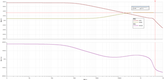
This thread has been locked.

If you have a related question, please click the "Ask a related question" button in the top right corner. The newly created question will be automatically linked to this question.

OPA855: Modify GBW of OPA855's SPICE model

Part Number: OPA855

Hi,together

  as shown in the datasheet of OPA855, the GBW is 8G, but in fact this parameter has a certain deviation, such as ±15%. As i want to conduct some worst-case simulation analysis, How can i change the GBW  in OP855's SPICE model.
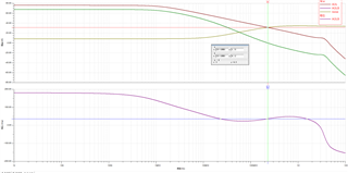
  • Also ,when I try to simulate the open loop GAIN, The open-loop gain curve intersects 0dB at 4.56G.  as i know ,The open-loop gain curve is not affected by the peripheral circuit. is there any error?

  • Hi,

    the open-loop gain is not constant but depends on many factors. One of them is the load resistance, for instance:

    https://www.eetimes.com/understanding-gain-and-load-dependencies-the-key-to-successful-rail-to-rail-op-amp-use/

    Kai

  • Hi Zhiyao,

    Certain parameters, like input referred noise, can easily be edited in the macro with a single line, but GBW is unfortunately not that simple. Is there a specific performance concern here with system bandwidth or are they just trying to get an idea of the error budget?

    Best,

    Sam

  • Hi Sam ,

    Recenty, we find the  output oscillation of our recently  op amp is even more serious. Through cross-testing, we confirmed that there may be some problems with this batch of chips. We suspect the bias of GBW in OPA855.

    According to the stability analysis of the op-amp, the phase margin is only 36.12°, but the amplitude of the oscillation is acceptable to us .So I guess that  the main pole's frequency of this batch of OPA855 has moved forward, leading to the decline of the phase margin, so that the  output oscillation of our recently  op amp is even more serious.

    In view of this ,I want to know the main pole deviation of different batches of chips, and how to simulate .

    Best,

  • Hi Zhiyao,

    that the GBW can be modifed by the change of only one paramter is a way too simplistic assumption here. These modern TI's Spice models are extremely complex and progressive. 

    The best remedy is to design the circuit in such a way that you have a phase margin with lots of headroom. This is way more elegant than trying to modify the Spice model.

    A phase margin of only 36° is way too small. Please show your schematic so that we can try to improve the phase margin.

    Keep also in mind that instability can also occur with improperly probing. Instabilty can also be the result of a poor layout (omtting of a solid ground plane, too big stray capacitances, too long copper tracks, etc), a poor supply voltage decoupling and the add of too big capacitive loads. So we would need to see a schematic, the layout and a photo of your setup to give good help.  

    Kai

  • Well Zhiyao, without your schematic hard to say on this - but 

    In a transimpedance design, the loop phase margin is mostly influenced by the dominant pole location in the model and the source C and feedback C. The dominant Aol pole is pretty simple in the model, the higher order poles and prop delay in the forward path is not but become more important for low voltage gain apps. here is the area in the model for the dominant pole, change C1 to test part to part in your circuit. Also, I think I used the Zt design to illustrate phase margin testing in this article, yes at the very end I went into a Zt design discussion for LG phase margin. 36deg is normally fine for a Zt design, but you should not be oscillating - in production, you need to fix that not ignore it. 

    https://www.planetanalog.com/stability-issues-for-high-speed-amplifiers-introductory-background-and-improved-analysis-insight-5/

  • Hi kai,

    Thank you for your advice. We plan to optimize the design in the next version, but considering the possible chip dispersion problem, we have to find out the situation.

  • Hi Zhiyao,

    Depending on the existing circuit topology, we can likely increase the overall phase margin to accommodate spec tolerances and remain stable. For the model adjustments you can try Michael's suggestions. Please share a schematic if you would like assistance adjusting the phase margin.

    Best,

    Sam