This thread has been locked.

If you have a related question, please click the "Ask a related question" button in the top right corner. The newly created question will be automatically linked to this question.

BUF802: Input Clamp diode connected to CLH, not VS+. Why?

Part Number: BUF802
Other Parts Discussed in Thread: , LMH6553

Hello,

The BUF802 is an interesting device to use on an oscilloscope input and has what appears to be a useful clamping feature to limit the swing into the following signal chain.

The input to the scope (when not using 50R termination) is typically a capacitive divider. e.g. a 10:1 probe could be 9M//10pF and the scope+compensation 1M//90pF. Often you need to look at the small part of a large waveform and this is where the clamping on the BUF802 would help. The input to the probe could be +/-50V which would be +/-5V at the scope input and then you could set the clamp levels to e.g. +/-1V to match the following signal chain.

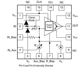
This works for the negative signal swing because the negative clamp diode is connected to VS-. Hence the scope input can swing down to -5V without any conduction on the clamps.

Setting CLL to -1V will not have any effect on the input signal.

However the positive clamp diode is connected to CLH (not VS+). So setting CLH to +1V will also clip the input signal to +1V + diode drop so about 1.7V. Doing this will cause distortion and offset due to charging of the input divider capacitors.

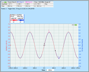
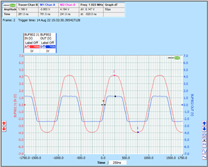
For example, testing with the BUF802RGTEVM using the composite configuration and removing L1 so input is high impedance. Then add a 3:1 capacitive divider (top 27pF//1M, bottom 81pF//333k) and drive with a 26Vpp 1MHz signal so the BUF802RGTEVM J1 input is +/-4.3V.

With CLH = VCC = 5V, CLL = VEE = -5V so there is no clipping I see Pin 2 VIN on the BUF802 (blue trace) closely matches the input signal on J1 (red trace).

Then reduce CLH from +5V to +1V. The input pin 2 on the BUF802 (blue trace) has been offset by approx 2V and both waveforms have become distorted. This is due to conduction in the positive clamp diode.

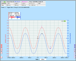
The offset has caused a pulse width error on the BUF802 output (blue trace):

So my question is why was the positive clamps diode connected to CLH and not VS+? It will cause input signal clipping, offset and distortion.

And if there is any plan to have a part where the positive clamp diode is connected to VS+

Thanks, Ken

  • Hello Ken, 

      That is a good question. I will ask the design engineer for more details on this choice. In general, this would affect the input clamping as you have shown. However, the device will act in a similar manner when the device sees an input signal less than VS-. Also, during standard operation, it is recommended that the clamp voltage applied at the CLH and CLL pins output signal is about 1.5V more than the expected peak output voltage which tracks the input voltage. 

      I will get back to you with more details. 

    Thank you,

    Sima

  • Thanks Sima,

    I look forward to the details.

    BR, Ken

  • Hi Sima,

    Did you have any feedback from the design engineer?

    Thanks, Ken

  • Hello Ken,

      Yes, sorry for the delay! It has to do with the operation of the internal NJFET:

    In relation with the datasheet’s block diagram:

    we see that the input (pin IN) goes to the gate of NJFET (channel is N-type and its gate is P-type). Now, for reliable operation of this NJFET, we need its gate-source (and gate-drain) to always be reverse biased – i.e. gate voltage not higher than the source voltage. Now, during clamping operation OUT gets clamped to CLH and we need to clamp the IN to CLH + Vdiode to keep the gate-source of input NJFET in the reverse biased region. For IN higher than this the gate-source can start going into forward bias which we don’t want.

    For negative side, when IN goes lower then CLH then the NJFET’s gate-source is getting even more reverse biased. So, we don’t need to do similar clamping to CLL – Vdiode, and there is regular clamping to VS-.

    Thank you,

    Sima

  • Thanks for the clarification Sima.

    Understood on the NJFET biasing. That is a shame as we really wanted to use the clamping in the BUF802, but also need to allow full +/-5V input swing without distortion on the capacitive divider. So will look at clamping further along the signal chain. Our present scope uses clamping on a LMH6553 but that has some issues on overload recovery, as discussed in this thread;

    https://e2e.ti.com/support/amplifiers-group/amplifiers/f/amplifiers-forum/715601/lmh6553-recovery-from-clamped-square-wave-shows-a-slow-decay/2639104#2639104

    We are considering as supply limited diff amp instead.

    Thanks for your help!

    Best regards, Ken

  • Hi Ken,

    in HF circuits a proper clamping can be achieved by using a "passive" diode clamp with a current limiting resistor and diodes to the supply rails. The trick here is to mount several high speed, low leakage diodes with low junction capacitance in series to decrease the capacitive loading and to prevent unwanted low pass filtering effects. If the clamping voltage is too high because of the many diodes in series, add a voltage divider behind the diode clamp to prevent the input voltage from exceeding the maximum input voltage of following chip.

    I have seen the legendary HSMS-2812 being used for this purpose.

    Kai