This thread has been locked.

If you have a related question, please click the "Ask a related question" button in the top right corner. The newly created question will be automatically linked to this question.

OPA541: Connection Question

Part Number: OPA541
Other Parts Discussed in Thread: TINA-TI

Hi Team,

I have a question regarding the OPA541P

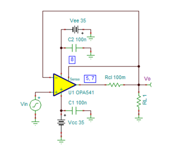
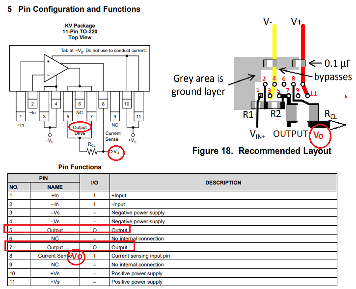
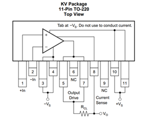
In TI data sheet, it shows:

    It seems that the current limit resistor will be connected between pin 5&7 and Pin 8. The output to external load will be at pin 8. Pin 8 is probably just a sense line that can sense the voltage across Rcl and determine if it should shut the device down. Current should flow out from pin 5&7 through the Rcl to the external load that is at Pin 8.

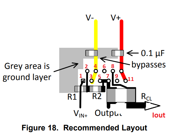
    However, another figure shows different:


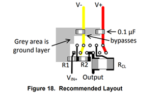
    The above shows that the output top external load with be from Pin 5&7.
    Which one is the right one. I had a feeling Figure 18 is wrong. With the above figure, there will be no current flow through Rcl.

Thanks!

Connor

  • Hi Connor,

    "It seems that the current limit resistor will be connected between pin 5&7 and Pin 8. The output to external load will be at pin 8. Pin 8 is probably just a sense line that can sense the voltage across Rcl and determine if it should shut the device down. Current should flow out from pin 5&7 through the Rcl to the external load that is at Pin 8."

    Your understanding is correct. The OPA541 output pins 5 and 7 connect directly to the RCL which is inside the feedback loop. Vo is taken from the other end of RCL which is also the sense connection that runs back to pin 8. You can see this illustrated in a TINA-TI test circuit diagram seen here:


    The layout shown in datasheet Figure 18 is incorrect. It was added years later to the OPA541 datasheet and apparently with the error already made. I'll need to let the PRAMPS System Engineer know about the problem so it can be corrected in the next OPA541 datasheet refresh.

    Thanks for questioning and bringing this to our attention.

    Regards, Thomas

    Precision Amplifiers Applications Engineering

  • I believe both drawings are correct and the only thing missing in Fig 18 is the Iout trace carrying high current to load - see below.

  • Hi Marek,

    The fact that Figure 18 is shows the OPA541 "Output" label on the left side of RCL is why I said it was incorrect. The datasheet Section 5, Pin Configuration and Functions table labels each of pins 5 and 7 as "Output." Your clarification showing the big Iout arrow on the right side of RCL is certainly correct, but I would like to see Vo label placed there so that it correlates with the Section 5, Pin Configuration and Functions pin diagram on page 3 which shows where Vo is connected.

    Regards, Thomas

    Precision Amplifiers Applications Engineering

  • Hi Thomas,

    The left side of RCL (pin 5 and 7) are consistently called OUTPUT while the right side (pin 8) is called Vo (Current Sense).  But I would agree that they should have shown Vo label in Fig 18 as well as Name Pin 8 Function Vo instead of calling it a Current Sense - see below.