This thread has been locked.

If you have a related question, please click the "Ask a related question" button in the top right corner. The newly created question will be automatically linked to this question.

THS4130: About Differential input voltage of Absolute Maximum Ratings

Guru 21045 points
Part Number: THS4130
Other Parts Discussed in Thread: THS4551, ADS9224R

Hi Team,


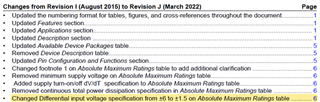
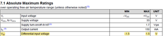
When changing from Rev I to Rev J, " Differential input voltage of Absolute Maximum Ratings" is changed from "±6V" to "±1.5V".

However, our customer designed using "±6 V". So it has a big impact.


-------

[Q1]

Is "±1.5V" a correct value, not a typo?


[Q2]

If "±1.5V" is the correct value, could you please let us know the reason for the change?


[Q3]

Is there a way to sort out "±1.5V" and "±6 V"?

For example, could you please let me know if it is possible to distinguish by TI label information?

(date code tec.)


[Q4]

They are designing for more than "±1.5V", is there a solution(workaround)?

-------


THS4130 datasheet

https://www.ti.com/lit/ds/symlink/ths4130.pdf

Regards,

Hide

  • Hello Hide,

    Could you share more details on how your customer has designed their system/circuit for +/- 6V differential input voltage maximum specification?

    I am thinking there is a slight bit of confusion around what this specification actually addresses.  When you have a moment, please take a look at a recent response I posted to a similar question on the forum:

    https://e2e.ti.com/support/amplifiers-group/amplifiers-internal/f/amplifiers-internal-forum/1134735/ths4551-differential-input-voltage-max-spec

    Your customer may be designing a system with a input signal +/- 6V differential, but the actual voltage present at the device pins likely does not swing +/- 6V.  My linked response will help explain further.

    Please respond and let me know if I can add clarity, or if you have a follow-up question.

    Best,

    Alec

  • Hi Alec-san,

    Thank you for your response.

    I can't see your URL information.

    Could you please let us know correct URL?

    By the way, Inside your URL is "Internal".

    So, I guess that I can’t see your ULR.

    If it is non-public information, please contact us offline.


    e2e.ti.com/.../amplifiers-internal/f/amplifiers-forum/1134735/ths4551-differential-input-voltage-max-spec

    Regards,

    Hide

  • Hello Hide,

    My apologies for the confusion; I did not catch the URL being internal.  I will relay the same post below for context:

    RESPONSE TO ABS MAX DIFF INPUT VOLTAGE SPEC FOR THS4551 FDA:

    ""

    Hello,

    Great question!  This is a common misconception of how amplifier specifications are interpreted, I will help you Slight smile.

    The absolute maximum specification for differential input voltage, in the case of the THS4551 being +/- 1V, refers to the maximum voltage between the IN+ and IN- pins on the amplifier.  This is not a spec unique to FDAs, but is present for amplifiers which will sustain damage if too much voltage is applied between the pins.  Back-to-back protection diodes usually assist with preventing this damage/failure; these are placed between the two inputs.  A high enough voltage will turn-on these diodes; if the voltage is not current-limited or the voltage is from an ESD event, the diodes can also be damaged.  

    Now, this is usually not an issue when discussing applications with customers, as under normal operation (specs like input common mode range, how close the amplifier can swing to the power rails, etc) the amplifier will keep its input pins close to the same voltage.  This is why the absolute max is such a tight range; normal operation results in very little difference between the voltages at the IN+ & IN- pins.

    Of course, this doesn't sound right!  How can input signals be larger than +/- 1V?  The 8.192Vpp voltage present in the ADC's datasheet, as well as voltages discussed as input sources to op-amp circuits across the industry, are voltages present at or before the gain resistors (ie, where the input voltage source is, say from a sensor).  The absolute maximum rating is for the voltage present at the input pins, IN+ & IN-.  Because of the 'virtual short' during linear operation of amplifiers, the voltage difference at the pins is normally quite small.  The voltages present throughout the resistor network can be much larger, and would be limited by other amplifier specifications, such as input common mode range & output swing limitations, to name a couple.

    In short, the actual voltage difference between the IN+ & IN- pins is very small.  The tight absolute maximum tolerance is actually a fairly good safety margin for safe operation, and under normal use (such as driving an ADC in the ADS9224R datasheet) will not come into play.  

    I really hope this helped you grow your understanding; please reply and reconnect if I did not make sense or you have additional questions.

    ""

    FOR HIDE:

    Hide, this explanation addresses important nuances for amplifier specifications.  In the above example, the question was on the +/- 1V abs max input differential voltage and how it can be true when the inputs in the attached input swing 8.192Vpeak-to-peak.  For your question, your customer may be using a system with +/- 6 Vpp inputs into the system, but your customer is likely not creating a +/- 6 Vpp difference between the IN+ & IN- pins of the amplifier.  

    Please let me know if you need anything else.

    Best,

    Alec

  • Hi Alec-san,


    Thank you for the detail information.

    I have aditional questions.


    --------

    [Q1]

    I understand that "±1.5V" is the correct value and it's not that "Differential input voltage" got worse.

    Could you please let us know the reason for the change?

    (For example, “Change to appropriate value” etc.)


    Until March 2022, "Differential input voltage" was ±6V.

    I would like to know why it suddenly became ±1.5V.

    ------


    [Q2]

    I understand that normally, we don't need to worry about "Differential input voltage".

    Because, ,if we use the appropriate input range, it will never exceed " Differential input voltage ".

    Is my understanding correct?


    <Excerpt of your information>

    - Now, this is usually not an issue when discussing applications with customers

    - The absolute maximum rating is for the voltage present at the input pins, IN+ & IN-.

     Because of the 'virtual short' during linear operation of amplifiers, the voltage difference at the pins is normally quite small.

    ------


    [Q3]

    Our customer use THS4130IDGKR and THS4131CDGKR.

    If I report their circuit and usage, could you check if there is no problem?

    *Currently, we are in discussion with them and are discussing how to proceed.

     If you agree, please let us know your email address offline.

    --------


    Regards,

    Hide

  • Hello Hide,

    I can certainly help with your questions!

    1. I have checked with my team on the datasheet changes.  I will connect with you offline regarding the datasheet revisions over email.

    2. You are correct, a normal application or well-documented use of an amplifier will not exceed this absolute maximum threshold of +/- 1.5V.  Scenarios where this could become an issue include when a large fast signal is injected into the amplifier, forcing the amplifier to slew at its maximum slew rate.  The driven input (where the signal comes in) has its voltage change faster than the amplifier can track with the other input pin, which is tracking the output via the feedback network.  This concept of slew rate and the input pins drifting apart is discussed in various training videos within the Operational Amplifiers section of TI Precision Labs.  The topics of Slew Rate, Current Feedback Amplifiers, Fully Differential Amplifiers, and Stability are important to this understanding.

    https://training.ti.com/ti-precision-labs-op-amps

    In a slew rate-limited scenario, a large signal drives one input of the amplifier, while the other input lags behind and cannot track the input signal.  The increasing difference between the voltage at both input pins is the differential input voltage.  While the output is lagging behind the input signal to create a difference between Vin & Vout, the more serious condition is how different the two input pins (IN+ and IN-) are.  You may recall the ideal linear model of an operational amplifier involves two main ideas:

    a) For an ideal voltage feedback amplifier, the current (I) in and out of the input terminals is zero amps.  This can also be thought of as both input terminals being very high impedance, which ideally is infinite.  In practice, the input leakage currents are very small (pico-amps to milli-amps) and the input impedance can be in mega-ohms.

    b) For an ideal amplifier, voltage or current feedback, there is a virtual GND between IN+ & IN-, the two amplifier inputs.  This means the differential input voltage between both pins should ideally be zero.  In practice, the input pins are very slightly different, with some amount of input offset voltage.  When an amplifier is driven to its limits or used out of spec, this differential input voltage will no longer be very close to zero, and could increase depending on what is happening in the circuit.  If the voltage difference between both pins is large enough, the amplifier will not operate in a linear range and could produce poor results and be damaged.  The limit of +/- 1.5V is set by the process technology and design, and exceeding this difference will begin to damage the device, or at minimum affect its ability to operate predictably.  

    If you & your customer are adhering to the recommended values and/or stay within the ranges stated in the recommended operation conditions, the circuit will be far less likely to encounter absolute maximum conditions.  The absolute maximum conditions, including the one for differential input voltage, exist to prevent misuse or damage to the amplifier and surrounding system.  

    3. I will connect with you via an e2e message to provide my email for schematic/circuit review.  

  • Hi Alec-san,

    Thank you for your prompt reply.

    I’m looking forward to hearing from you for "1".

    Regards,

    Hide

  • Hello Hide-san,

    I will await your response.

    Best,

    Alec

  • Hello Hide-san & forum,

    Discussion of THS4130DGK datasheet revisions has been moved offline in order to more directly support customer questions.  Discussion of how abs max differential input voltage affects amplifier operation has been sufficiently concluded in this thread.

    For additional persons curious about Rev I to Rev J datasheet changes, please reference the public releases on TI DFAB & SFAB closures.  The migration of support and manufacturing of devices such as the THS4130DGK to newer TI processes has been a product-line priority and is reflected by these datasheet revisions.

    Please contact the HSAMPs team if you require specific information on these items.  A product change notice has been sent for various packages to existing customers who require such notice, including on the DGK package. 

    For new and prospective users of the THS4130, this information is supplemental and the current datasheet reflects the current product.  

    Best,

    Alec