This thread has been locked.

If you have a related question, please click the "Ask a related question" button in the top right corner. The newly created question will be automatically linked to this question.

INA333: INA333 output is ~0V and not meet my expected during measure a serial thermistor

Part Number: INA333

Hi, dear product line  engineer.

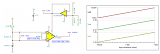
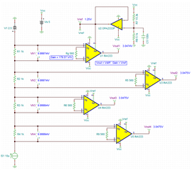
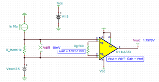
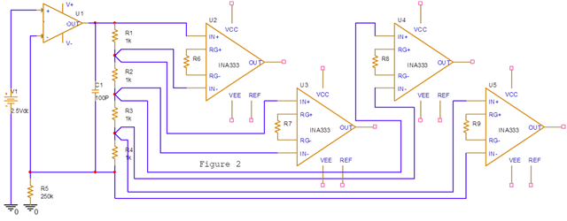
my customer use iNA333 to measure the voltage of 4-serial thermistor. the schematic as below. the current is 10uA, thermistor is 1k and Rg is 560-ohm. then the expected output of INA333 should be 1.796V. however, my customer said: all the output of INA333 is near 0V when he mount all 4-INA333. the output seems correct if he just mount U4 and U5 or U4 or U5. I checked the schematic and datasheet. seems customer's design meet specification of datasheet and no incorrect.

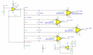
then I do a simulation. the result is the output of INA333(U5) meet my expect perfect if I remove U2,U3 and U4 and just keep U5. the exactly situation for U4. but U3(remove U2,U4,U5) and U2(remove U3,U4,U5) could not pass the simulation.  

could you please help to figure out the root cause? thank you very much!

regards,

Bill 

  • Hi Bill, 

    Could you specify the Vcc, Vee and Vref  used by the customer? I can simulate the circuit for you. 

    Best,

    Raymond

  • the VCC is 5V and VEE is GND, VREF also connected to GND. thanks for supporting!

    regards,

    Bill

  • Hi Bill, 

    The issues are: you have approx. Vcm = 2.5Vdc, if the V-to-I circuit is configured properly, but you may also need to establish Vref voltage, see the simulation. In the simulation below, I configure the Vref = 1.25Vdc, since the circuit is designed with 5Vdc single supply rail. 

    With Vcm = 2.5Vdc and Vref = GND = 0V, your Vcm vs. Vout linear relationship is shown below. 

    With Vcm = 2.5Vdc and Vref = 1.25Vdc, the Vcm vs. Vout linear relationship is shown as follows. With the configuration, your input signals are widen (now included the negative differential input voltage as well),  Vcm and Vout ranges are increased in the linear operating range. You may decide what is the best Vref for your application.  

    Regarding to the above tool, you may download the Analog Engineer's calculator in the link below. 

    https://www.ti.com/tool/ANALOG-ENGINEER-CALC

    Enclosed is the simulation of the circuit. 

    INA333 thermistor 11102022.TSC

    If you have additional questions, please let me know. 

    Best,

    Raymond

  • hi, Raymond.

    thank you for supporting!

    no. 2.5V/250k=0.00001=10uA. not 10mA.

    regards,

    Bill

  • Hi Bill, 

    yeah, I goofed.

     The simulation is correct. Please let me know if you still have issues. 

    Best.

    Raymond

  • Hi, Raymond

    for the bottom 1k thermistor, I can simulation it correctly. but for the top and second top 1k thermistor, the simulator could not run. could you try it again? BTW, do you have wechat? you can add me by 13816050423. we can talk it by wehcat for details. thanks.

    regards,

    Bill

  • Hi Bill, 

    Could you send me the Tina file? Which op amp did you simulate for V-to-I converter?

    Best,

    Raymond

  • I use Pspice for Ti and an idea constant-current source and set the current to 10uA. below is my file. I use "bias analysis' function. for the bottom and second bottom 1k thermistor, the simulation can run and get expexted result. but simulation could not run for top and second top 1k thermistor.  

    INA333.DSN 

    regards,

    Bill

  • Hi Bill, 

    You need to establish the correct Vcm mode and pay attention to the input range of INA333, which is shown in the calculator below, see red circles, Vmin and Vmax and Vout_min and Vout_max range for a given Vcm and Vref voltage. 

    Here is the simulation. 10uA represents the current source from V-to-I converter. Vcm = 2.5Vdc represents the input common mode voltage, since you are using the single supply rail. Also pay attention to Vdifferential_input = Vin+ - Vin, and the the transfer function. 

    INA333 with 4-thermistors 11102022.TSC

    If you have additional questions, please let me know. 

    Best,

    Raymond

  • Hi, Raymond

    according my calculation, even the common input voltage is 2.5V, the first stage amplifier in INA333 still not saturation with ~89.3 gain. the output of first amplifier should be ~3.433V. the reference is just for output offset. so what is root cause?

    BTW, I could not run  simulation successful in Pspice for TI even I add reference with 1.25V.

    regards,

    Bill

  • Hi Bill, 

    I simulated the whole schematic and I do not see the issues. 

    As you indicated, the upper and lower Vcm voltages are approx. 2.5Vdc. If the differential input voltage is Vdiff = 10mV, the Vout = 10mV *89.3 V/V + 1.25V = 2.143V (assume Vref = 1.25Vdc).

    Also, please let me know what op amp your customer is using in V-to-I converter. Here is an example and will need to check for the loop stability. 

    INA333 + OPA333 current source 11112022.TSC

    the reference is just for output offset. so what is root cause?

    Vref is NOT simply an offset at Vout. It also affect the input differential voltage as seen in the image below. with Vref, it opens up the circuit differential signal swing on top of Vcm mode voltage. I have provided you with the tool and please check it out the effect. Pay attention to the marked fields as you change IA's configuration parameters. Pls change one filed at a time and then do the input and output comparisons. 

    Best,

    Raymond

  • Hi, Raymond

    yes, you are right. the output of INA333 is Vo=Vd(1+100k/560)+Vref. the Vref limtied differential input voltage if differential voltage is negative and power supply with single positive voltage.

    customer V-to-I converter is MAX4238.

    for the customer application, the Vd always positive, and then output of INA333 should be always positive too, even ref=0.  for this example, the Vd=10mV and Gain=179.57. Vref=0. so the output should be vo=1.796V. but why some INA333 has no output?

    anyway, I will try debug the circuit once I received the PCBA board from customer.

    thanks for your supporting!

    regards,

    Bill

  • Hi Bill,

    so the output should be vo=1.796V. but why some INA333 has no output?

    If the Vcm is placed at 2.5Vdc, Vdiff = 10mA, Vref = GND = 0Vdc, you should get Vout as simulated below. Please measure the input and output voltage at the the PCB, and relate these measurement to me. I do not know how the circuit is actually configured on the PCB. 

    Best,

    Raymond

  • customer--INA333AD_4.TSC

    hi, Ramond

     attached is customer schematic. the simulation result is not correct. I compare your file and customer file and find the INA333 is different between two files. replace INA333 in customer file with INA333 in your file. then the simulation succesful and meet my expected. it has no relationship with REF as I point out ago. I make REF to GND and the simulation runs good in your file. so could you please share where are you get the INA333 or do you update the pspice module of INA333? thank you very much!

    regards,

    Bill

  • Hi, Raymond

    I now know the reason. you should use Pspice model from TI web. customer and me use Pspice model from TINA. customer simulation also succesful and meet my expected after I update INA333 with Pspice model from TI web. so the root cause is INA333 model in TINA is incorrect. thanks for your great supporting!

    regards,

    Bill