This thread has been locked.
If you have a related question, please click the "Ask a related question" button in the top right corner. The newly created question will be automatically linked to this question.
Hi Team,
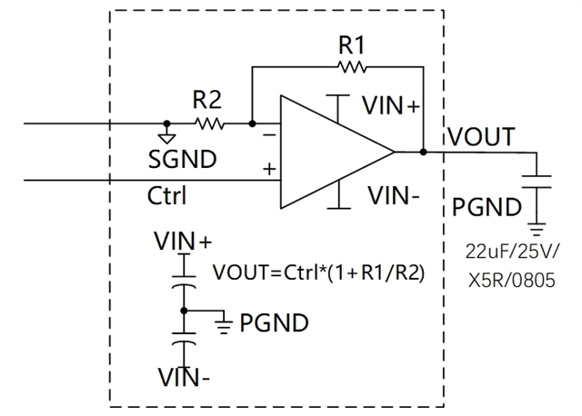
I am making a voltage controlled voltage source with OPA549, the following is the schematic diagram, I encountered two problems during use:
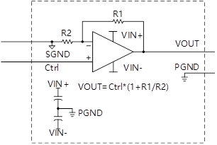
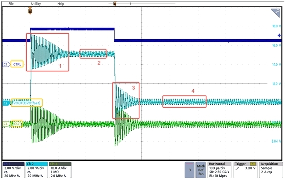
1) The power-on sequence of VIN+ and VIN- seems to have requirements: under no-load condition, the Ctrl terminal is always shorted to SGND. If VIN+ is powered on first, before VIN- is powered on, VOUT will output a voltage close to VIN+ ; Similarly, if VIN- is powered off first, VOUT will output a voltage close to VIN+. As shown below
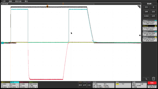
Black: VIN+; Blue: VOUT; Rose: VIN-
But that voltage is pulled down to zero by a certain amount of resistance (in the order of hundreds of ohms). Why does the power-on and power-on sequence affect the output? This is not reflected in the D/S.
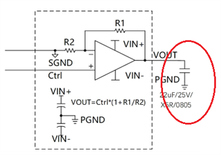
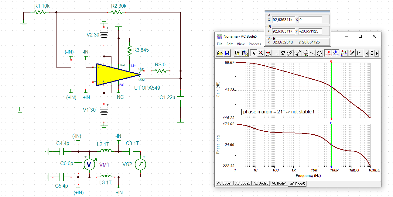
2) There will be some ringing and stable low frequency oscillation when the output is connected to no-load or capacitive load. These oscillations will also be damped by a certain amount of resistive load, but is there any other better method?
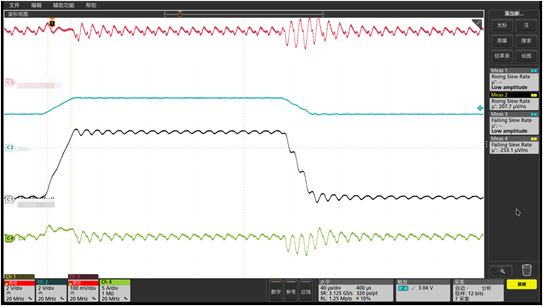
Blue: Ctrl; Black: VOUT; Green: IOUT
-A
Hi Albert,
The OPA549 like nearly all op amps is designed to use positive and negative supplies that are applied and come up to level in the same manner, at the same time. When one supply comes up to level before the other it may force the op amp into a non-linear condition where the common-mode voltage, or another parameter's range is exceeded. Additionally, when one supply lags the other unintended, internal current paths can be formed that result in unexpected behaviors.
Most often op amps are not characterized for power supply sequencing behaviors. The possibilities are limitless. Sometimes, more controlled start-up behaviors are had by adding power diodes or TVS diodes from each supply pin to ground. If one supply comes up earlier than the other the normally reverse-biased diode on the other supply becomes forward-biased providing a current path for the supply current.
Regarding the ringing:
Regards, Thomas
Precision Amplifiers Applications Engineering
Hi Thomas,
Please see my reply below. Thanks!
Hi Albert,
Thanks for the responses regarding your OPA549 circuit. The circuit gain, supply bypassing and application circuit appear okay. A genuine TI OPA549 would be stable in the circuit and not exhibit ripple on its output waveform unless it is coming from something else in the circuit.
Thanks, Thomas
Precision Amplifiers Applications Engineering
Hi Thomas,
Hi Albert,
the OPAmp oscillates because of a too high capacitive load at the output which ruins the phase margin and causes instability. See the chapter "output stage compensation" of datasheet.
Kai
Hi Albert,
As Kai pointed out, the configuration is driving a capacitive load directly, which it will degrade the phase margin in OPA549 and cause op amp instability and oscillation at the output.
Please provide us the input, output and BW design requirements in the OPA549. We have to find a way to compensate the OPA549's feedback loop in order to drive the large capacitive load.
Please also check out the video clip shown below.
Best,
Raymond
Hi Albert,
please explain why you connect a such high capacitance directly at the output of OPA549. Please explain what you are planning to do.
Kai
Hi Albert,
I am going to close this inquiry. If you have additional questions, please let us know.
Best,
Raymond