This thread has been locked.

If you have a related question, please click the "Ask a related question" button in the top right corner. The newly created question will be automatically linked to this question.

XTR111: VIN floating input, not connected question

Part Number: XTR111
Other Parts Discussed in Thread: OPA188

Hello,

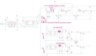
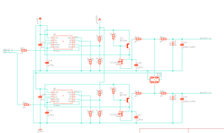
I'm using XTR111 for a PCB I've built. My board can have voltage or current output. For voltage output the output of my DAC is connected to an op-amp circuit, for current output the DAC is connected to the input pin of my XTR111 circuit. This is done use jumpers.
Actually I also have jumpers for the OD (output disable) pin of the XTR111, those are connected when the board is in voltage mode output.
I would like to remove the OD jumpers. So leave the XTR111 always on.
My question is: if I don't want to use the current output, what if the input pin of XTR111 (namely VIN) is left floating, so unconnected? Do you find any issue on that?

Thanks!

  • A high-impedance input should never be left floating (with or without OD). In particular, the input voltage might go above the valid range.

    A weak pull-down resistor would help. (The input impedance is 2.4 GΩ, so 1 MΩ would be enough.)

  • Thanks!
    So, I've I've understand well the schematic attached should work. (removed OD, and added resistors to pulldown input on the 2 op-amp voltage outputs and the 2 XTR111 current output.
    Is that right?

  • Thank you!
    I'll check it on my sample board. If all ok I'll apply to next board and mark it as "This resolved my issue".

  • Hi Davide,

    too high source impedances at the inputs of OPAmp and XTR111 can cause stability issues. So, I would decrease the pull-down resistances to 100k.

    Then I would add a series resistance of 2k5 between the pull-down resistor and the inputs of OPAmp and XTR111 (see figure 46 of datasheet of XTR111). And finally a low pass filtering cap should be added behind this series resistor to signal ground. This heavily decreases the source impedance at high frequencies and massively enhances stability. But it also serves as a low pass filter to remove HF-contents (coming from the DAC) at the inputs OPAmp and XTR111 and by this at the output cabling. Without these filters common mode noise can make the board fail the CE radiation testing.

    Kai

  • HI Kai, Clemens,

    Thank you for your help.

    Hi Davide,

    I agree with Kai and Clemens, adding the 100k pull-down resistor at the XTR111 input and RC filter to remove HF-contents.

    Another recommendation, if you are not using the XTR111 regulator, please connect the REGS and REGF pins together and add a 470nF bypass capacitor as shown on Figure 45a on p18 of the datasheet.  This is to ensure stable operation of the device.

    Thank you and Regards,

    Luis

  • Thank you all.

    I've finally decided to go for a DPDT. Because the op-amp is a unipolar to bipolar convert, and i prefer to output it a 0V when disconnected, so I've to make a voltage divider at +5VREF/2.
    - when volt out is not connected, the op amp is connected to a voltage divider formed by 2 x 10k resistor. One pulled up to +5VREF, one to GND, so that output is almost 0V.
    - when current out is not connected, the VIN pin of XTR111 is connected to GND, so that output from XTR111 is 0mA
    Also:
    - added the 2k resistor at VIN pin of XTR111 as figure 46 of datasheet.
    - connected REGS and REGF pins together and add a 470nF cap to GND
    Removed:
    - the pulldown resistor
    Not done:
    - filter from DAC to voltage or current out circuit.
    Filtering circuit, what's the cutoff you suggest?
    - thinking about putting a 1k resistor between DAC and op amp, and a 220pF to GND for a ~700kHz simple filter
    - thinking about putting a 100pF to GND after the 2k resistor of the XTR111 input pin for a ~800kHz simple filter

    Find new schematic below

  • Hi Davide,

    The corner frequency of the filter will depend on the frequency range of the EMI signals that the circuit will be exposed on the application, how much EMI and noise needs to be filtered out, and/or the EMI test/certifications that your module will be submitted to.  For example, EMI testing generally has a low band range of 30MHz to 200MHz and a high band range of 200MHz to 1GHz.  Conducted RFI is often tested in the low-frequency range around 150kHz to 80MHz.  

     For example, let’s say you decided to set the filter corner frequency at around ~50-KHz, per your application EMI filtering requirement.

    The OPA188 is a zero drift or chopper amplifier. Since the OPA188 is a chopper, the input bias current does exhibit periodic switching transients. This input bias current transient become transformed to a voltage offset when the bias currents flow through the high value circuit resistors. Therefore, chopper amplifiers like OPA188 may need to match the equivalent input impedances between the op-amp positive and negative input terminals in order to eliminate the commutation of the IB spikes across unmatched input impedance.  In the example circuit below, I matched the equivalent impedances in the inverting and non-inverting terminal to 10.7k | | 20.5K | | 22.6k = 5.36k on each input terminal to reduce the effect of the chopper amplifier IB spikes.  The capacitances seen at the non-inverting and inverting input terminals are also matched.   I tentatively set the capacitor to 550pF for a filter corner frequency to 53-kHz in this example:

    From the XTR111 perspective, the device input has relatively low input bias current, 15nA typical, so you could use a resistor from 2kΩ to 10kΩ range without adding significant error.  For example, if you decided to use the same filter as above, you could use the same 5.36kOhm and 550pF for a corner frequency at ~54kHz.

    Thank you and Kind Regards,

    Luis

  • Thank you Luis!

    I'll improve my design with your suggestions.

  • HI Davide,

    Thank you.  

    Best Regards.

    Luis