This thread has been locked.

If you have a related question, please click the "Ask a related question" button in the top right corner. The newly created question will be automatically linked to this question.

TLV9354-Q1: About bypass capacitor capacity between V+ and V- terminals

Part Number: TLV9354-Q1

Hi there,

About bypass capacitor capacity between V+ and V- terminals,

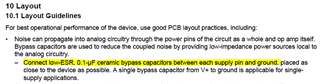
The datasheet seems to recommend a capacitor value of 0.1uF.

Is there any problem when setting the capacitance of this capacitor to 1uF?

Best regards.

  • No. Low impedance (i.e., small package and short traces) is more important than the exact value.

  • Thank you for your response.

    This IC is used for 10kHz signals.
    What impedance should it be?

  • If one capacitor has a smaller package, you should choose that one. But otherwise, 100 nF or 1 µF does not really matter.

  • Hi Keiji,

    because the TLV9354-Q1 is a rather fast OPAmp and shows a slew rate of 20V/µs (which is quite a lot), placing decoupling caps close to the OPAmp as shown in figure 10-4 of datasheet is mandatory. Here it is important that the inductances seen be the OPAmp supply voltage pins become minimal. This means that the decoupling caps should come in small packages and should be connected closest to the OPAmp while the ground terminals should sit on a solid ground plane.

    Keep in mind that the layout in figure 10-4 assumes a solid ground plane in another layer below the component layer with all the ground pours and ground fills on the top layer being connected to the below ground plane by dozens of vias! Without the solid ground plane and the vias the ground fills on the top layer would be isolated from each other!

    In most of my OPAmp circuits I use 470nF / X7R / 0805 decoupling caps connected to each OPAmp supply voltage pin. But any other capacitance between 100nF and let's say 1µF would also be ok. But choose a cap in a small package, like 0805 or RM5 or so, Do not use a big axial electrolytic cap or another dino for this.

    This is the standard decoupling configuration. But in circuits with very high gain (microphone amplifier, or esle) you may want to increase the decoupling capacitances to improve the supply voltage noise filtering. Then you can mount a SMD tantal or a small aluminimum electrolytic cap in parallel to this 470nF / X7R / 0805 decoupling cap. Something from 10µF to 100µF should do then. To improve the supply voltage filtering a small resistor of 10...100R may be mounted in series of these decoupling caps to form a simple low pass filter.

    The same is true when a heavier load has to be driven by the output of an OPAmp (headphone amplifier, or esle). Then an increase of the decoupling capacitances by the above paralleling can also be helpful. The bigger decoupling cap helps to provide a bigger reservoir for the bigger load currents. Even a small resistor can be added as discussed above to improve the "isolation" between the headphone amplifer and the rest of circuitry. But in order to minimize the voltage drops caused by the hgiher load currents much lower resistor values should be chosen, something between 1...10R or so.

    Kai

  • Hey Keiji, 

    I usually reference these two blog posts by Tim Claycomb: 

    The basics: How to layout a PCB for an op amp

    How to lay out a PCB for high-performance, low-side current-sensing designs

    All the best,
    Carolina