This thread has been locked.

If you have a related question, please click the "Ask a related question" button in the top right corner. The newly created question will be automatically linked to this question.

TLV6710: Resistor calculation unclear

Part Number: TLV6710
Other Parts Discussed in Thread: TINA-TI

Hi, I'm not able to get the correct resistor values based on my understanding of the parameters of this device.

My requirements: TLV6710 configured as Window comparator with OutA and B tied together  OutA/B "0" when Vmon between 0V and 2.4V.   When Vmon rises above 2.4V, OutA/B is "1".  When Vmon goes above 2.7V, OutA/B becomes "0".  When Vmon drops to 2.6V and below, OutA/B is "1".  See diagram pasted below.

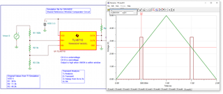
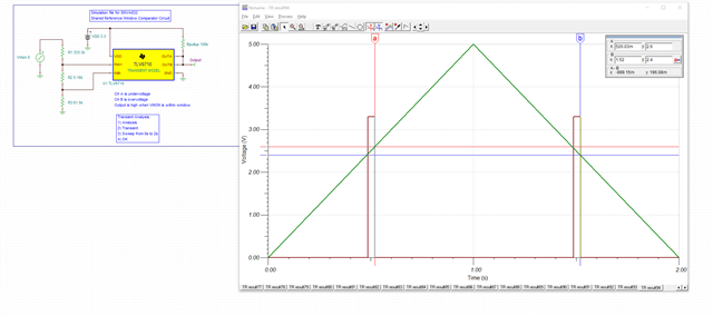
I ran the TINA-TI simulation on your website and got the R values experimentally, but I can't reconcile with my calculations.  Much of the confusion is the definition of, and the relationship between these variables:

VIT+(INA), VMON(UV_HYS), VIT-(INA), VMON(UV), VIT+(INB), VMON(OV), VIT-(INB),VMON(OV _HYS).  

I think the relationship is the following from the datasheet: 

VIT+(INA) = VMON(UV_HYS), VIT-(INA) = VMON(UV), VIT+(INB) = VMON(OV), VIT-(INB) = VMON(OV _HYS).  This is from 9.1.1 ("The highest accuracy threshold voltages are VIT–(INA) and VIT+(INB), and correspond with the falling undervoltage flag, and the rising overvoltage flag, respectively."). The sticking point are the words "correspond with".  Please correct me if I'm wrong.

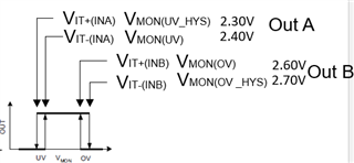
Also, the example in the datasheet is confusing, specifically why VIT+(INB) and VIT-(INA) are 0.4V (I see nothing in the example requirements that point to 0.4V and I can't figure out how to derive it).

This 0.4V seems to be contradictory to multiple places in the datasheet that indicate that these values should be in the window range VIT+(INB) around 26.4V and VIT-(INA) should be near 21.6V (for example, section 6 says when INB exceeds VIT+(INB), OUTB is driven low).

Please help me sort this out, preferably showing the calculations with my requirements.

Here's a screenshot of my simulation.  I don't think it exactly lines up with my requirements, but it is close.  Much closer than what the calculations give me.

  • Hi Scott,

    Thanks for reaching out. I understand its a lot to take in with all the variables. But let me try to keep it simple.

    0.4V is the internal reference of the comparator. It is what the inputs are being compared to internally. But since there is already internal hysteresis of about 5.5mV, then the point  at which the output toggles isn't always exactly 0.4V but perhaps shifted a little by 5mV, depending on which way you are traversing through on the input. See the specs of the reference and hysteresis in the EC table of section 7.5 as well as the timing diagram in Figure 20 where it shows the output is toggling. 

    The resistor divider network allows you to monitor higher voltages and then dividing it down to near the internal reference of 0.4V. 

    For the calculations, V MON (OV) and V MON (UV) are your actually target overvoltage and undervoltage conditions. V IT+ (INB) and VIT- (INA) can be taken from the ec table, in this case 0.4V. Then Rtotal you can assume some large value resistance.

    If 2.4V and 2.6V are your target OV and UV conditions, and you choose Rtotal = 400kohm, here is what you would get from the equations.

     tlv6710window.TSC

  • Thank you.  That is so much clearer how you explain it.  I see now how V IT+ (INB) and VIT- (INA) can be derived with more deep analysis, but it would be so much more helpful if the data sheet could be updated to say what you stated.

    At the minimum, under 9.1.1 app information, state for Formula (3):

    "where VMON(UV_HYS) is the target voltage at which an undervoltage condition is removed as VMON rises. AND where VIT+(INA) is equal to 0.4V"

    and for formula (4):

    "VMON(UV) is the target voltage at which an undervoltage condition is detected AND where VIT-(INA) equal to 0.4V"

  • One more side question, what is "too small" in 9.3 statement: 

    Do not use pullup resistors that are too small, because the larger current sunk by the output then exceeds the desired low-level output voltage (VOL).

    I can't reconcile that statement with a calculation, not enough information. The output pin current is 10mA max, so is this saying to choose resistors high enough to not saturate that current sinking through the chip?  With 5V rail, 5V/0.01A = 500Ohms. Or is this not what the note is saying?  I chose 10k pullups to 5V rail, and need to know if I need to replace those.

  • Hi Scott,

    Thank you for the feedback. We will look into making this clearer in the datasheet.

    If the pull up resistor is too small, then the current sunk would be very large which would start to raise your VOL levels and increase overall power dissipation of your system. See Fig 14-15 for the relationship btwn output voltage and output current. Yes, 500 ohms would be the minimum, however, although it might not damage the comparator, it will raise the VOL levels. Generally we like to recommend 1mA or less of sunk current. A 10k pull up to 5V is good. 

    See Section 3.2 of this app note: Application Design Guidelines for LM339, LM393, TL331 Family Comparators (Rev. B)

  • Ok. Thanks for your very timely help.  I have a prototype wired and working as expected.  Thanks!

    Scott