Other Parts Discussed in Thread: OPA818
Hello!
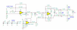
I'm testing the design mentioned in
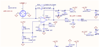
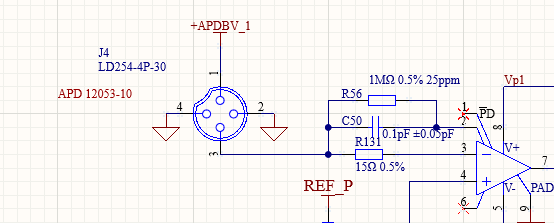
And the final circuit diagram:
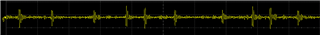
And I fnd the output of the OP657 has a noisy output. The maximum value will be around 40mVp-p. (I used a axial cable with 100Ω isolate resistor, and the waveform is same as the result of ADC output ,so it's credible)
I've confirmed all the power supply, the ripple/noise are all below 3-5mV.
And then I removed the feedback capacitor but it still kept the same.
Then I changed the gain resistor to 1k and 100k, then the result:
1k - 0.5mVpp pretty well;
100k - 1.47mVpp
400k - 9.6mVpp
It seems there's some current noise on the input side of OPA657 and amplified.
And I doubt with the environment so I also have another channel of Scope using same axial cable connected to nothing but near the PCBA (NC in the below waveform).
So I guess the spikes are from the environment.
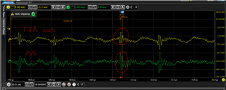
But drop the spikes, there seems to be a sine waveform on the output of TIA.
I did the phase margin simulation and also tried different feedback capacitor, but they didn't work.
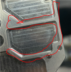
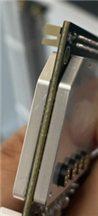
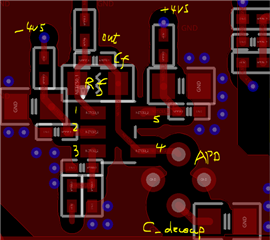
And there's trace without sold mask to install the steel shielding case, but I'm still waiting for the delivery.
Before I get the sheilding parts, what else can I try?
Thanks!
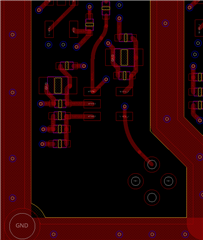
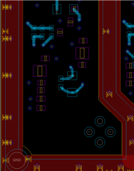
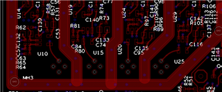
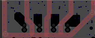
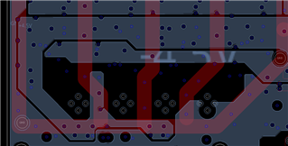
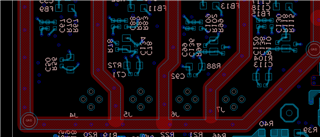
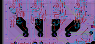
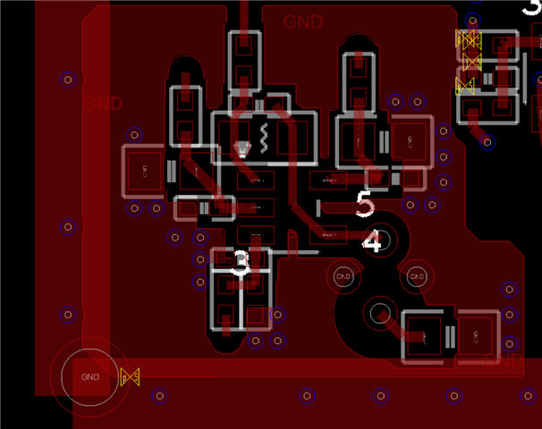
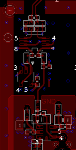
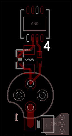
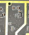
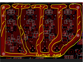
Layout: