This thread has been locked.

If you have a related question, please click the "Ask a related question" button in the top right corner. The newly created question will be automatically linked to this question.

OPA357: Suitable signal treatment discrete system?

Part Number: OPA357

Hello,
In order to develop a way to treat a input signal to be sampled by a 12 bit ADC, the following circuits were designed:


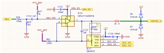
For the reference voltage, we will use this configuration:


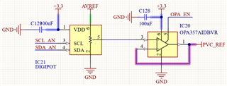
Description of the situation:
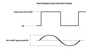
1. Input ignal: The system need to be able to capture two types of signal (from a BLDC or PMSM motor phase), and for each type the signal can vary its amplitude as shown:
    * Sinusoidal: Max Vpp = 60V with zero offset and min Vpp = 6V with zero offset;
    * PWM of max frequency 200kHz: Max amplitude = 60V and min amplitude = 6V, all with min level ideally at 0v.
2. ADC: 12bit with sampling rate of 0.5uS (Max desirable).

Questions:
1. The circuit was designed to allow the system to vary the offset accordly to each situation. this offsed is applied through the digipot from the 2nd figure. In this configration, is the OPA357 suitable to this application, as the offset could be amplified and thus clamp at the upper limit?
2. If so, by varing the 2nd figure digipot wiper the system should only virtually apply an offset to the signal. Is this correct?
3. For a bandpass configuration, should C125 be removed and then place a capacitor in parallel with D7?
4. Will the R58, R59, C124 and R57 cause a phase delay or a signal distortion?

I would like to ask you to answer these questions to know if this PN is suitable for our application.
We are totally open to suggestions and corrections (please consider suggesting improvements to this system)

Thanks for your attention!

  • Hi Emanuel, 

    I want to clarify my understanding of your circuit. Right now your maximum input is 60Vpp in one condition and 54Vpp in the second correct? I am concerned as that currently results in a input voltage maximum condition of 2.68Vpp. With what appears to be a minimum gain of 4.4 V/V, the amplifier output will certainly saturate and clip at your large input voltage conditions. Is that your desired behavior? 

    Your general technique of adjusting the offset to center the signal depending on the input common mode should work. I am just concerned by the output limitations with such a large input voltage. 

    You can create a simple band-pass filter by adding a low-pass to the output. You will need some series resistance on the output for that to work. Also, I would suggest at least adding a small series output resistance regardless to help isolate the capacitance of the diodes from the output of the amplifier so they do not affect stability. 

    Any capacitor in the signal path will affect the phase. The exact change in phase will depend on the the component values and any other circuitry. I would simply suggest simulating the total phase of the signal path. Also, just to be clear, the phase delay of the signal path is not the same as the phase related to the amplifier stability. 

    You can get some small distortion from thick film resistors and certain capacitors with large voltage swings, but that is usually only a concern for applications that require very low distortion. What is your target distortion performance for your circuit? 

    Regards, 

    Jacob 

  • HI Jacob,

    1. Actually I want to be able to capture PWM signals with different amplitudes, where the extreme situations would be: PWM @ 0-to-60V (max case) and PWM @ 0-to-6V (min case).

    2. For the case you mentioned to be a gain of 4.4V/V min with input signal max level of 2.68Vpp: indeed the op amp will saturate. My ideia was to shift the offset (PVC_REF) in this case and then make signal excursionate around PVC_REF. Doing so, if I'm right, the output signal would be Vout max = PVC_REF +  ( 2.68/2 * gain ), that's what I meant.

    3. In "You can create a simple band-pass filter by adding a low-pass to the output. You will need some series resistance on the output for that to work. Also, I would suggest at least adding a small series output resistance regardless to help isolate the capacitance of the diodes from the output of the amplifier so they do not affect stability." you meant to change the J6 for a resistor? (if possible, could you draw your suggestions just to make sure? )

    4. Ideally the performance would be around the ADC capabilities, e.g., 12 bits @ 0.5uS (sampling time), so if all noise and distortion fall within the LSB error, would be enough.

    Our main concern is applying the offset to the signal so that the ADC could capture the entire shifted signal, as the ADC get non-negative values between 0 and 3.3V.

    Do you see any problems with the R58 being 10's of kOhms? Any concerns about higher values for this component?

  • Hi Emanuel, 

    If I am understanding correctly you want to add a DC shift to the amplifier to reduce the maximum output voltage under the 60V input case? This would work but when the signal returns to 0V the op-amp will then saturate to the negative side. It would probably be easier to add a switable attenuation to the resistor network before the amplifier and just switch that to attenuate further with the large signal case. That would allow you to maintain good SNR when the input is small but also not saturate. 

    For the filter, yes replacing J6 with a resistor and selecting appropriate R and C values will add a low-pass after the amplifier.

    R58 value should not hurt at all other than its contribution of noise. 

    Let me know what you think of my proposal of using a switched input attenuation as I believe that would solve most of your issues. 

    Best, 

    Jacob 

  • Hi Jacob.

    Not only reduce the voltage when under the 60V input case but in all cases. The following image shows the two types of signal the system should capture:


    The offset needs to be applied in both cases because:
    1. For PWM: although all the PWM input signals have always a zero voltage as its lower voltagem, some effects effects caused by the motor inductance and PWM switching can add a negative voltage. So adding an DC offset to this input signal will make the system capable of capturing all the real signal without clamping at the lower voltage.
    2. For the sinusoidal (PMSM): the signal from the PMSM motor phases will show up as an AC wave, so the system needs to shift it so that the ADC can capture entirely the signal.

    About your comment, I have some points to check:
    1. You said that at zero the system would saturate. The saturation at the zero volts input could be mitigated using the PVC_REF control, done by the reference voltage cascaded with the opa, in the second image in my original post, isn't it?
    2. About the ideia of controlling the system with switchable resistor: It coud work for the 60V case but take an intermediate value for the pwm amplitude of let's say 30V, the gain would be too high or too low, so I would loose resolution. This solution discretizes the signal well for the 6V case and for the 60V case, but for some point between them could create a low SNR.
    Please correct me if I am wrong.

  • Hi Jacob, 

    Could you please check the last message? 

    Thanks for your help again! 

  • Hi Emanuel, 

    Thank you for the waveforms, that clarified my understanding. Apologies in the delay in response. 

    I think your offset scheme should be okay, but you'll still need to take care of the output swing problem. The switched input attenuation should work as your worst case SNR will always be at the lowest input signal level even if you increase the attenuation at higher input voltages. The increased attenuation will reduce the SNR but it will still be better than your worst case value at the lowest input. 

    Here is a table I put together showing an example with just a sinusoidal input and assuming approximately 38.2 uVrms input noise from the amplifier. At 16 volts I changed the attenuation from 0.045 to 0.012 to ekeep the output under 3.3V at the 60V input. As you can see the SNR at 6Vpp input is still the lowest in the system even though we added some extra attenuation at 16V inputs. 

    Input (Vpp Sinusoid) Input (Vrms) Attenuation (V/V) Attenuated Signal (Vpp) SNR (dB) AMP Out (Vpp)
    6 4.24 0.045 0.268 50.5 1.18
    10 7.07 0.045 0.447 52.7 1.97
    15 10.61 0.045 0.671 54.4 2.95
    16 11.31 0.012 0.192 54.7 0.84
    30 21.21 0.012 0.360 57.4 1.58
    40 28.28 0.012 0.480 58.7 2.11
    60 42.43 0.012 0.720 60.5 3.17

    Best, 

    Jacob