Other Parts Discussed in Thread: OPA320, OPA357, ADS7945, ADS7946
Hello to whom this may concern,
This is the description of the situation:
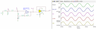
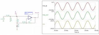
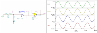
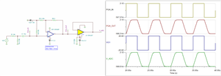
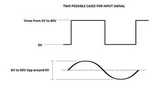
1. Input ignal: The system need to be able to capture two types of signal (from a BLDC or PMSM motor phase), and for each type the signal can vary its amplitude as shown:
* Sinusoidal: Max Vpp = 60V with zero offset and min Vpp = 6V with zero offset;
* PWM of max frequency 200kHz: Max amplitude = 60V and min amplitude = 6V, all with min level ideally at 0v.
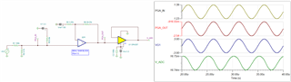
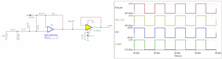
Both signals are represented below:
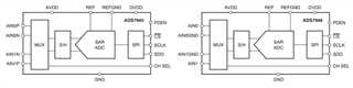
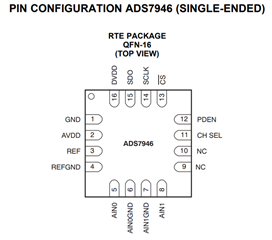
2. ADC: 12bit with sampling rate of 0.5uS (Max desirable).
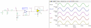
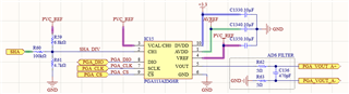
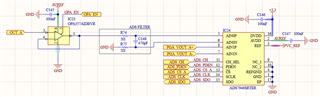
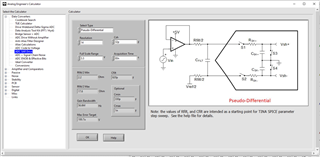
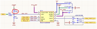
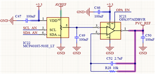
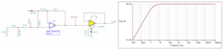
To make possible to treat the signal, the following circuit is proposed: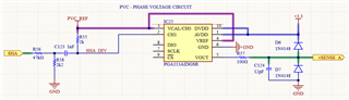
Knowing all of this, we have some questions:
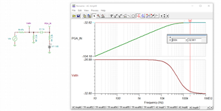
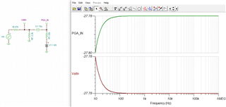
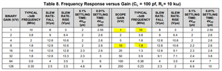
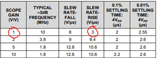
1. What would be the real closed-loop BW of this system for PGA gain 1 to 10 ?
2. Is this real closed-loop BW compatible with the 12 bit ADC @ 0.5uS sampling rate ?