This thread has been locked.

If you have a related question, please click the "Ask a related question" button in the top right corner. The newly created question will be automatically linked to this question.

TLV9002: Error in Measuring the Voltage

Part Number: TLV9002
Other Parts Discussed in Thread: LM358A, LM224, TINA-TI

Hi,

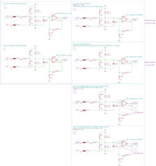
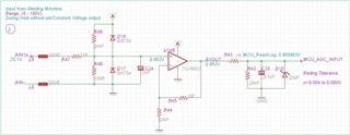
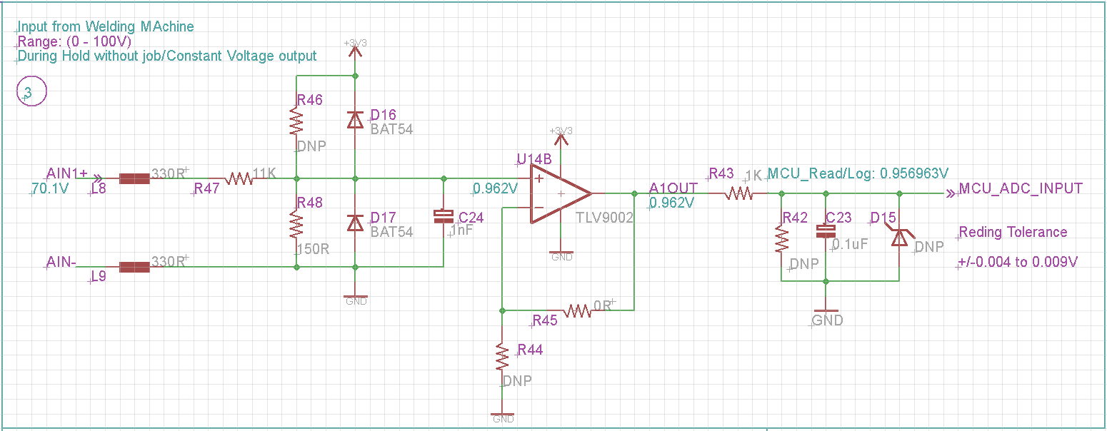
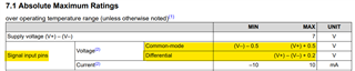
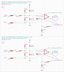
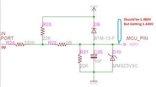
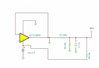
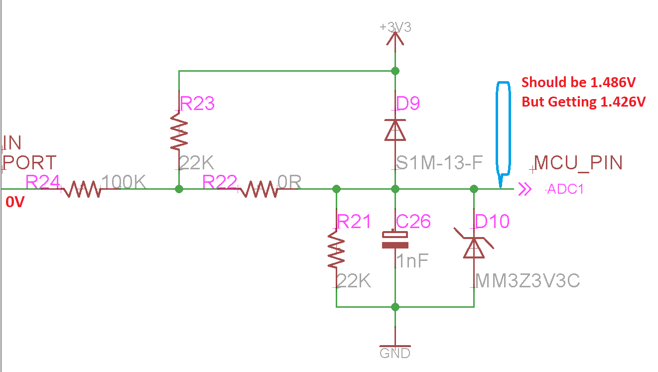
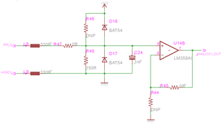
Existing circuit is working fine to measure the voltage,. But in one application it failed to measure the Weld (DC Voltage) voltage from the Welding Machine. Output of the Amplifier will not be same as IN+. (Added 3MOhm series resistor to  AIN_1). Weld Voltage range ill be 0-100VDC and it can able to read from third party DC energy meters.

PFA the schematic and kindly advise if any modification required in the circuit to measure the voltage.

Thanks and regards,

Naveen K

  • Hi Naveen,

    Is the sensing design using the TLV9002 or the LM358A?

    Can you share screenshots of a working and non working measurement?

    These details will help us understand what may be causing the issue.

    Best,

    Jacob

  • Dear Jacob,

    Thank you for the response.

    Please find the updated and tested Circuit and kindly advise for the below query.

    1. Circuit 1 and 2 will be works as expected even on the MCU reading/Printing side as well.

    2. Circuit 3 will be fine till Amplifier Output and minor Acceptable Tolerance on MCU reading/Printing the value.

    3. Circuit 4 will be fine till Amplifier Output, but little more Tolerance on MCU reading/Printing the value. Need your advise to reduce the Tolerance.

    4. Circuit 5 and 6, Till Amplifier Input will be Fine. But the Amplifier Output was very high compare to the input. We don't know how the output and input will be different even it's a Voltage Follower. Kindly Advise to resolve the issue. 

    Thanks and regards,

    Naveen K

  • Hi Naveen, Thank you for the additional details here. 

    The TLV9002 is a RRIO(Rail to Rail Input-Output) amplifier, and we are seeing non-linearity as the buffer is required to output close to the V- supply. 

    What is the amplifier driving?

    This looks like an output limitation caused by the amplifier running out of output swing.

    The output swing from the supply rail is dependent on output current, as seen here: 

    Can you confirm if the amplifier is driving any load? This will help us understand if the issue is output related.

    Please let me know if you have any questions.

    Thank you,

    Jacob

  • Dear Jacob,

    Amplifier not driving any load. Amplifier output is connected to Microcontroller through 1K series resistor, just to measure the Voltage. Amplifier VDD=3.3V and VSS=Ground. Not connected any negative source.

    The measure voltages with respect to the nodes are specified n the circuit,  kindly advise for the last query no. 3 and 4.

    Thanks and regards,

    Naveen K

  • Hi Naveen, 

    Thank you for these details,

    I figure you are using the microcontroller for its internal ADC which samples the voltage on the output of the amplifier. Are you also measuring the voltages in blue with a DMM?

    For query 3, this is more of an ADC related characteristic. If we look at the voltage output, the amplifier has an accurate output relative to the input. The ADC however is reading a value which is different than the amplifier output voltage. Are you using an RC filter before the ADC of the microcontroller? this is the best way to get accurate ADC samples. Here is an example design for a buffer driving an ADC with an RC filter after the amplifier:

    For Query 4, I suspect this is related to output swing. Can you confirm you are using TLV9002 in this circuit? I remember LM358A was mentioned earlier in the thread. Also, is this circuit in DC steady state when you are taking these values? If this is not in a DC setting, the amplifier output may be delayed when compared to the input.

    Do you have the ability to connect a negative voltage to the supply rail of the part for testing purposes? If you do, I would connect -.2V to this node with VCC remaining the same. This would help us understand if this is output related. If the V- amplifier connection is directly to GND then this type of test will not be possible.

    Best,

    Jacob

  • Hi Jacob,

    Thank you for the information.

    Please find the circuit including Amplifier output to Microcontroller input. We using RC Filter (1KOhm and 0.1uF), We using Microcontroller which having internal ADC. 

    Query3:

    We using RC Filter (1K and 0.1uF) as shown in circuit. We are making 50 samples and printing average of 50 samples. One more observation is that, reading will be more accurate for constant/stable input from any sensor/Supply. But it will be more difference on reading/print during input voltage will be changing frequently like during Machine operations going ON(Like Welding Job).

    You can also see the Junk Log printing during Machine operations, But there is no Junks during Machine is on standby. You can see both the logs.

    Suggest if any changes is required in the circuit as well as on samples/firmware side to get accurate reading.

    Query 4:

    We using TLV9002IDR now, but we also using LMV358AIDR when TLV9002IDR no available. Hope both characteristics are same only.

    All the Circuit (1 to 6) are same except the Input side Voltage divider will be different on Circuit 5 & 6. All circuits are just connected to Microcontroller through RC Filter as shown in the above circuit to measure the voltage. The Supply Voltage and Measurable Voltages are DC only, Even Machine operates in DC only.

    Query 4.1.

    For Circuit 5 or 6, If the OPAMP analog input from the DC power supply, it will works fine (OPAMP input=OPAMP Output). If i connect the same OPAMP analog input to the Machine voltage source to measure the voltage, then OPAMP Input=0.3V & OPAMP Output=0.71V even during Stand-by. During Machine Operations the OPAMP Input=0.106V and OPAMP Output=0.0983V. Why this Input to Output Voltage Difference?

    Query 4.2.

    You can see the Circuit in this new post, OPAMP VCC=3.3V and VSS=GND. As explained same circuit Input from Power supply will gives Opamp Input=Output, and same circuit input connect from Machine Opamp Input=0.3V and Output=0.71V. If necessary, i can able to give -.0.2V to OPamp input from the DC Power supply, hope it will not works. Kindly confirm.

    Query 4.3

    What is Output Swing? Hope this means, If OPAMP output driving any load and if driving current insufficient it will cause Output voltage difference. Hopefully the output Voltage will drop down. Is this right?

    Thanks and regards,

    Naveen K 

  • Hi Naveen,

    Thank you for the great details, this helps significantly in debugging the system. 

    Query 3: 

    This seems unique. I cannot imagine this is issue you are seeing is related to hardware. Is it possible that the welding machine is emitting electromagnetic waves which interfere with the operation of the microcontroller?  I typically associate "junk data" like that to be caused by interference during digital communication. It might be worthwhile to test this by shielding the sensing system and microcontroller. If this is not related to EMI, I am not sure where to look next. This type of error could also be software related.

    For Query 4.1, this makes me think there may be grounding issues in the system. The DC power source works, but the machine input of equivalent voltage does not. Do you have a low impedance ground connection to the sensing node? 

    For query 4.2: we do not need to test the VEE at -.2V anymore. You proved that the output is capable of swinging close to V- in the DC power source testing during condition 5 and 6.

    Query 4.3: Correct, this is exactly how output swing works. It is clear that while his looked previously like a output swing issue, the test you completed with the DC power supply proves this issue is different in nature. 

    This is a very unique issue, I am not sure why this particular problem is happening only in condition 5/6.

    We have experienced strange problems like this in the past when it comes to grounding with Analog and digital circuits. 

    Is there any source impedance looking into the voltage sensing of the machine? I am trying to understand what other differences exist between the welding machine and the DC power source. 

    Please let me know if you have any questions.

    Best,

    Jacob

  • Hi Jacob,

    Thank you for the information.

    First we will close the Query 3 (Circuit 1-4) and later will come for Circuit 5-6.

    Yes, No Hardware issue on the Circuit 1-4 to measure the Voltage. Machine will cause Interference. But it not impacting the device. Example if i connect Other sensors/DC Power supply to the OPAMP input and keeping the Device in the Machine and even if the device powered up from Machine source, There is no junks on the print logs. I think it's issue from the Analog signal ground.  Actually, Machine Source Ground and Measurable signal Ground will be different. This Measurable Ground having more fluctuations during the Operations like the voltage varies from 20 to 30V even some spikes 45V even though we have adjusted the Output Voltage(Measurable) 23V. I think this connecting device ground and signal ground causing the interference on printing the logs? Kindly suggest to resolve this issue.

    Thanks and regards,

    Naveen K

  • Hello Naveen,

    Today is a US holiday , expect a reply tomorrow. 

  • Hi Naveen,

    Thanks for the details. I tis good to know that the sensing circuitry is working perfectly fine. 

    This can sometimes be a consequence of sensing high voltages or high currents. PCB layout can be very impactful in system performance. 

    Is the analog signal ground the same ground which is connecting to the op amp VEE supply?

    I would agree, this ground fluctuation is the likely culprit for the problems you are experiencing. 

    How are you connecting your grounds together? It is important to look at current loops, and identify where the current is flowing. Clearly, it is flowing through significant impedance to create this significant voltage spike. 

    Are you using ground pours on your board? I have never seen voltage spikes this high on a GND plane before. 

    Best,

    Jacob

  • Hi Jacob,

    Thank you for the information.

    You can see in the circuit, Machine Analog Ground is connected to our Device ground through 330Ohm Ferrite Bead. Our Device Ground, OPAMP Ground(VEE) is same. Come to PCB Layout, it's a 4 layer board 1,4- Signal layer, 2-Ground layer, 3-Power(3.3V)-Layer.

    I think no issue on the Layout design, because if we connect third part Boards between our Device and Machine, everything will be fine. If we skip third party board and directly connected to measuring point, then there is a junks/Interference.

    One more thing, there is one more measurable voltage from the Machine(0-2V), its Ground and Measurable(0-100V) ground (This interference conversation) is different in the machine. If we connect only other measurable voltage (0-2V), device measures voltage without interference. If we connect (0-100V) measuring voltage then causing Interference. Hope we can realize there is no PCB/Design/Layout issue right?

    Other thing is that, Spikes are generated by Machine only during Operation and it's unavoidable, because it's operating nature. We need to avoid the interference. Kindly suggest how to isolate the Machine Analog Ground and please advise any other possible way's?

    Thanks and regards,

    Naveen K

  • Hi Ronald,

    Nice to hear from you and hope you doing Good!.

    This circuit is suggested by you 2 years back and working fine for many applications, Thank you for your support.

    Recently, We are noticing interference(MCU printing Junk logs) issue while connected to one Welding Machine to measure the Voltage. During Machine stand by: No-Junks, During Machine Operation: Junk printing Logs.

    Thanks and regards,

    Naveen K

  • Hi Naveen,

    I appreciate your patience as we debug this issue. 

    I believe the problem exists in that the machine ground is shifting the analog ground such that the ADC is being placed in an undesired state: this then outputs junk data. 

    If the machine ground is truly spiking up to 30-45V relative to analog ground, this significant voltage shift will probably be enough to cause issues in the system. 

    Ground shift is caused by current flowing through an impedance, relative to another ground. 

    This may be caused by the ferrite bead connecting Ain- to GND. I think the ferrite is a good design choice for attenuating high frequency noise, but can we replace L9 with a zero ohm resistor for testing?

    This zero ohm resistor swap will confirm if the ferrite bead is the reason for the ground shifting. A consequence of this will be higher noise on the GND rail, but this may help with reducing the amplitude of the spike.

    Alternatively, we could maybe look to use an isolation amplifier, but these are far from inexpensive devices. Effectively, this type of device would isolate the machine ground and the analog ground from one another, while still allowing for a sensed voltage to be transferred over the isolation barrier. 

    Please let me know if you are able to test the zero ohm resistor experiment. 

    Thank you,

    Jacob

  • Hi Jacob,

    Sorry for the delay in response due to the unavailability of the resource.

    We also tried with Zero Ohm Resistor, results are same.

    One more thing we noticed is that, may be our TTL to USB converter causing interference, we changed the converter and now there is no interference and working as expected.

    Kindly advise, Connecting Machine Load Ground and our Device Ground is the right step? or do we need to isolate or add any other circuitry in between these Grounds? Kindly suggest with the best solution to avoid any interference issue in the future.

    Thanks and regards,

    Naveen K

  • Hi Naveen,

    Thank you for trying the 0-Ohm test. 

    It is great to hear that you were able to debug the problem. It is interesting that the TTL to USB was the source of the problem.

    Grounding can be a complex topic, and there are many different methods which can be used to realize an effective grounding solution. 

    Firstly, you should look at your return current paths, these will help you understand what can be localized on a certain ground plane, and what may have to pass from GND(A) to GND(B).

    One method of connecting different grounds is to use a star ground. Effectively, this will connect the grounds at one central point, forcing return currents to pass through this single point. 

    Some designers use ferrite beads, others use 0-Ohm resistors or traces segments to connect the different grounds on the board. 

    Ultimately, the goal of these methods is to reduce the likelihood of ground loops causing shifts in the performance of your system. 

    When laying out a PCB, try to keep components of similar ground close together. This will effectively reduce the path length of ground return currents.

    Also, if you are using ground planes on different layers, be sure to stitch the pours together with vias. 

    I am not sure how the layout of the board looks, but your method of using a ferrite bead should work for connecting the grounds. 

    Thank you,

    Jacob

  • Hi Jacob,

    Thank you for the information.

    We use 4-Layer stack and in that 1 layer dedicated for ground. Outside(Machine Analog) Ground directly connected to Ground Layer throug 330R Ferrite bead. No Star point/ground has used here.

    1. Normally we use Ferrite Beads in series for all the Device input ports like L8 and L9 in these circuits to reduce the interference. Kindly advise how to choose the right Bead value?
    2. Also, normally we use RC(R43 and C23) before the MCU pin. Kindly advise how to choose the RC value for better accuracy?
    3. If in some cases we may use R42 to act as Potential Divider. In this case, still R43 and C23 functions as an RC filter or we may need to add one more resistor between R42 and C23 to functions as RC filter?
    4. Right now Zener Diode (P/N: MM3Z3V3C) D15 is made as DNP. Because wrong readings happen if the diode is present. Am not sure the reasons but I think this diode will help to avoid MCU damage if voltage exceeds VCC. And also i have noticed in some circuits are used the general Rectifier diodes an higher side like D16 in this circuit. Kindly advise which type of diode will be best on the MCU ADC input pin side.
    5. Hope TLV9002 supply should be 0-5V only and Analog Input should not be Negative Voltage range should be same as supply. TLV9002 can not be used in Inverter Application right? But LM224N supply voltage can be -15V to +15V and Analog IN can be -15V to +15V.

    Thanks and regards,

    Naveen K

  • Hi Naveen,

    Jacob is currently out but will back on Monday. Would you be able to wait for his reply till then? 

    Best Regards, 

    Robert Clifton 

  • Hi Robert,

    Thank you for the information.

    Sure, we will wait.

    Thanks and regards,

    Naveen K

  • Hi Naveen,

    Thank you for understanding. 

    Though I think I can help with a few of your questions. Below I'm focusing on Question 5.

    Hope TLV9002 supply should be 0-5V only and Analog Input should not be Negative Voltage range should be same as supply.

    To clarify, you are saying the supply voltage of the TLV9002? The TLV9002 can only operate with a supply voltage range of 1.8V to 5.5V. Beyond those ranges we cannot guarantee the device's performance. 

    The analog input can only go a little beyond the supply voltages of the op amp. If you go further, that would cause the input ESD diodes to begin conducting. 

    TLV9002 can not be used in Inverter Application right?

    You can use the TLV9002 in an inverting application. This isn't a problem. 

    1. But LM224N supply voltage can be -15V to +15V and Analog IN can be -15V to +15V.

    Not quite. The LM224 has an input common mode limitation of VCC-2 that needs to be taken into account. 

    Best Regards,

    Robert Clifton 

  • Hi Naveen, 

    I agree with all of the points that Robert made. 

    1. Ferrite beads look resistive at high frequencies. The best way to size the ferrite involves looking at the manufacturer impedance vs. frequency plot. Your circuit also forms a resistive divider, so this can help attenuate the high frequency signal. 

    2. This RC filter acts as a charge bucket for the ADC sampling. The idea is that this capacitor will allow the SAR ADC to have the internal sampling capacitor charged by C23 without significant change in C23 voltage. The series resistor improves the stability of the system, and prevents significant overshoot on the output. I recommend using the Analog Engineer Calculator for evaluating the best RC values for your ADC. Alternatively, you can also refer to the microcontroller datasheet for recommended values. 

    3. Yes, you can use this resistor for voltage dividing, but it will change the filter cutoff frequency. 

    4. That is correct, the MM3Z3V3C diode is being used for protecting the ADC from overvoltage. You can use a similar protection scheme(BAT54) on the input of the ADC if you would like. Here is an app note covering an example: Circuit for protecting ADS131M0x ADC from electrical overstress

     Please let me know if you have any questions,

    Best,

    Jacob

  • Hi,

    Thank you for the support.

    1. To size the Ferrit Bead, Can you please explain with some example? For example if it mentioned that,  220Ohm @ 100MHZ and Part No, "MPZ1608S221ATA00". How size the ferrite bead for this above discussed OPAMP Circuit?

    2. We are Using CC3220MODSF12MOBR MCU. Kindly suggest the RC Value? (We use 12bit ADC, 10sample/Sec)? Kindly suggest, Any Document on to Select RC Value?

    3. RC with Potential Divider, Yes Cutoff frequency will be change, could you advice How we can Calculate RC value for this case?

    4. BAT 54 required on both pulled up and down side like D16 and D17 right?

    5. ESD Diode: can we use normal Schottky Diode or specifically need to use TVS Diode only?

    Thanks and regards,

    Naveen K

  • Hi Naveen,

    1. For specific advice on ferrite beads, I recommend leveraging the manufacturer for specific advice. In my experience, the best way to size a ferrite bead involves selecting a bead which attenuates the frequencies you are most concerned for. For example, if I was concerned about 100+MHz noise coupling into my sensing system, the ferrite below would work well. 

    2. Here is the app note on the specific ADC you are using: SimpleLink Wi-Fi® CC32xx ADC. If you are only sampling once every 100ms, the RC values are perfectly fine the way they currently are.

    3. The resistors will look like they are in parallel from an AC perspective, making the cutoff frequency equal to 1/(2*pi*(R43||R42)*C23)

    4. Correct, to both sides ideally.

    5. TVS diodes are always a good component for additional ESD protection. 

  • Hi Jacob.

    Thank you for the information.

    Regarding to the circuits 1,2,3,4 we will implement the same.

    As discussed earlier, Regarding to the Circuit 5 or 6, Kindly advise the reason to have a INPUT and VOLTAGE voltage reference on the OPAMP? Even its a Voltage Follower.

    Thanks and regards,

    Naveen K

  • Hi Naveen, 

    This is most commonly implemented to protect against input or output limitations in the amplifier.  

    For example, if I have a buffer with an input range from 0-1V on the input, I would ideally expect to get 0-1V on the output. As we know, amplifiers have a finite input and output range, so the output would likely not be able to swing all the way down to 0V if we have a grounded negative supply rail of the amplifier. 

    To prevent this output swing limitation, some customers intentionally introduce a DC offset on the amplifier. Continuing our example, if I have the same input signal with a .1V reference, my output range will now be from .1V to 1.1V. I have the same analog scaling, just with a DC offset. 

    Since you are only driving an ADC, you should not have to worry too much about output wing limitation. 

    As we can see from the TLV9002 datasheet, you can expect the output to get reasonably close to the rails depending on load current: 

    Thanks,

    Jacob

  • Hi Jacob,

    Thank you for the information.

    I think this is not a DC Offset issue. and output is not in linier with input. Even if i connect variable power supply, amplifier works fine as a voltage follower.

    I will explain on the source side. There is a machine output voltage it is connected to transformer primary (CT) and Secondary-output of the transformer is connected to machine side amplifier circuits. We are measuring the voltage at the Primary/input side of the transformer pins. Measured DC resistance of the Transformer primary pins was 1Ohm.

    I doubting that, our Amplifier inputs connected to Transformer primary and amplifier input impedance will be very low ( measured DC Resistance=1Ohm). This 1Ohm impacting the issue on the voltage follower? kindly advise.

    Thanks and regards,

    Naveen K

  • Hi Naveen, 

    I agree that this is a case of non-linear output with the input.

    I do not think the source impedance is causing problems, the amplifier input is effectively high impedance when compared to the secondary side winding resistance. 

    Could this be grounding related? It is good that you have tested the amp with a variable supply, this confirms that the error is in fact something with the source side. How are you terminating the transformer? Are there high currents flowing through the transformer? I assume the transformer connects between AIN+ and AIN-

    What is the primary to secondary turns ratio of the transformer?

    As a test, can you disconnect the machine output from the primary of the transformer, and replace this with a equivalent signal source like a function generator or power supply? This may help us understand if the transformer is causing the non-linearity.

    Thank you,

    Jacob

  • Hi Naveen,

    It's been several weeks since we heard back. I'm going to assume that this issue has been resolved and close the thread.

    Best Regards, 

    Robert Clifton 

  • Hi,

    Thank you for the support and sorry for the delay in response.

    We have implemented the circuit and working fine. But we are not getting the calculated Voltage as expected. There is two cases.

    Case1: Voltage Devider circuit IN Port connected to OPAMP Output and ADC1 connected to MCU Analog Pin:

    We connected Devider In Port to Ground and the expected Voltage on ADC1 Pin or MCU Analog pin should be 1.486V, but we are getting 1,.426V.

    Case2: Voltage Devider circuit IN Port connected to Ground and ADC1 pin of the Devider circuit connected to OPAMP INPIUT(IN+)

    We connected Devider In Port to Ground and the expected Voltage on ADC1 Pin should be 1.486V, we are getting 1,.478V.

    Case2 will be acceptable due to some Resistor Tolarence but why in Case 1 we are getting too less Voltage?

    Thanks and regards,

    Naveen K

  • Hey Naveen,

    How are you figuring out your "expected voltage"? Is this a mathematical estimate, or a measured value with a DMM?

    In case 1, it sounds like you are connecting the amp to the divider circuit , but this is causing the voltage measurement to be different than what you expect.

    Are you shorting the amp output to ground? it sounds like you are connecting both the in port and the amp output to ground.

    Can you probe the in port voltage in case 1? also probe the MCU_PIN voltage if possible with a DMM. 

    Thanks,

    Jacob

  • Hi Jacob,

    Thank you for the information.

    In my old post, Mr. Ronald has suggested the circuit and Calculator. even same calculations has comes in the simulator also. So, am considering the simulator output as expected Voltage. 

    Tested with DMM again and results as follows.

    Yes, we are connected OPAMP Output to Ground, it also means IN-PORT of Divider is connected to Ground. In this case Voltage at MCU pin will be 1.422V.

    If the OPAMP Output was not connected to Ground, then the MCU pin Voltage will be 1.426V.

    We suppose to get 1.486± 0.01V Right?

    Thanks and regards,

    Naveen K

  • Hi Naveen.

    I do not think it is a good idea to connect the amplifier output to ground when the amplifier has a grounded VEE rail. This is because this voltage is outside the output swing range of the amplifier, and this can cause large amounts of current to flow in the output stage transistors. 

    We can see this in your TINA-TI simulations as the amplifier output can only swing to a minimum voltage of about 20mV.

    What is the function of shorting the amplifier output to ground? In my eyes, this circuit is buffering an input voltage and scaling it to work with the ADC input range.

    1.486V output assumes that the resistors are perfect, and that the 3.3V supply is exactly 3.3V.

    In the case of the output not shorted to ground, we see the MCU pin voltage is 1.426V. The buffer circuit will attempt to recreate this voltage on the output of the amplifier. This means that some of your error is likely coming from resistor tolerance and the magnitude of your 3.3V rail.

    Please let me know if you have any questions,

    Best,

    Jacob

  • Hi Jacob,

    Thank you for the information and appreciated your quick response.

    In application we wont short OPAMP output to ground. for troubleshooting purpose and to get confirmation prospective we have connected manually to ground only.

    There is no resistor tolerance for this circuit, all resistors are +/-1% tolerance and even we can expect only 0.01V tolerance. and VCC=3.28 Only. But we getting 0.06V difference which equal to 0.5V on the Total Voltage. This is affecting to our calculation and in calculation we are getting negative voltage.

    With the same VCC and Resistor/Circuit, if we connect in the OPAMP Input side we are getting as we expected with 0.005 negligible Voltage. So kindly advise the reasons which causing issues.

    Thanks and regards,

    Naveen K

  • Hey Naveen,

    Thanks for the clarification on the output. I recreated your circuit in TINA-TI, I agree that this would be a large difference in value for 1% resistors. 

    Just to confirm, you are using the amp to drive the ADC, right? In your previous post, it sounds like the ADC is connected to the MCU-pin, which comes before the buffer. 

    In your previous post:

    Case1: Voltage Devider circuit IN Port connected to OPAMP Output and ADC1 connected to MCU Analog Pin:

    We connected Devider In Port to Ground and the expected Voltage on ADC1 Pin or MCU Analog pin should be 1.486V, but we are getting 1,.426V.

    Case2: Voltage Devider circuit IN Port connected to Ground and ADC1 pin of the Devider circuit connected to OPAMP INPIUT(IN+)

    We connected Devider In Port to Ground and the expected Voltage on ADC1 Pin should be 1.486V, we are getting 1,.478V.

    Case2 will be acceptable due to some Resistor Tolarence but why in Case 1 we are getting too less Voltage?

    It sounds like case 1 and 2 are different circuit configurations, am I mistaken?

    Best,

    Jacob

  • Hi Jacob,

    Thank you for the information.

    Divider Circuit is same for both the cases.Just location is different. In case1 Divider Circuit is present after the OPAMP and in Case2 Diver circuit is present before the OPAMP Circuit.

    You can Refer Below Circuit for Case2 and R1,R2,R3 which forms as Voltage divider. So Voltage Divider Circuit will be same for both the Case 1 & 2.

    Thanks and regards,

    Naveen K

  • Hi Naveen, 

    Thank you for confirming the configuration, this helps me quite a bit. 

    Voltage Devider circuit IN Port connected to OPAMP Output, Devider In Port to Ground

    Case 1 (without diodes): Divider input = Amp output = GND

    This circuit does not converge in simulation for me, please let me know if I implemented the circuit different than you expected. 

    I think case 2 is the better approach for driving the ADC, this circuit would not use the amplifier in a helpful way.

    Case 2 also protects the amp input from high voltage unlike case 1.

    Thanks,

    Jacob

  • Hi Jacob,

    Thank you for the information.

    Found that,Issue is with the Zener Diode D10 (Partnumber: MM3Z3V3C). If i remove the Zener Diode, I will get 1.478V which can be expectable. 

    But am struck here, Why Zener diode causing issue. Purpose of this diode is to protect the MCU from >3.3V. We are using 3.3 V Zener Diode and the voltage was 1.486, How diode is drops the Voltage from 1.486V to 1,426V. But, if i increase the IN-PORT Voltage (Zener Diode present), ADC1 voltage will increase for >3V.

    Please see the diode datasheet in the given link and advise the reason causing this voltage drop issue.

    https://www.onsemi.com/pdf/datasheet/mm3z9v1c-d.pdf

    Thanks and regards,

    Naveen K

  • Hi Naveen,

    Thank you for debugging this, I had failed to consider that the D10 diode would be conducting slightly. 

    My theory: the Zener diode will not have a sharp conduction knee when compared to alternative diodes. This lack of a sharp clamping point is causing the conduction to start before you are expecting it.

    D9 protects against voltages higher than 3.3V, D10 should protect against voltages less than GND.

    It might be necessary for us to select a different diode for D10. Do you have access to any other diodes for testing? I would throw a BAV199 diode in place of D10 if you want a quick way to confirm the theory that the Zener is the problem.

    Best,

    Jacob

  • Hi Jacob,

    Thank you for the information.

    We don't have BAV199. Hope BAV199 is also a Schottky diode.   

    We Tested replacing with 1N4148WS and BAT54JFILM. Both Working as expected as 1.476V. It was 1.424V when diode MM3Z3V3C present.

    Purpose of the Zener Diode is to protect the MCU pin, but here Why can't we use Zener Diode? Kindly advise with better sollution.


    Thanks and regards,

    Naveen K

  • Hi Naveen,

    You are welcome to use whatever diode makes the most sense in you application, the Zener may not always be the best option. 

    The Zener has some unique characteristics related to its IV curve, this is likely the reason you are experiencing the voltage drop.

    I do not think we need to use a Zener diode here, we could swap the Zener for a Schottky diode here instead assuming we use D9 for overvoltage protection.

    The idea is that D9 will conduct to the V+ (3.3V) rail whenever there is an overvoltage event. D10 would forward bias for negative voltages. 

    In your current configuration D10 would reverse bias in the Zener region for voltage at Vz around 3.3V terminating to GND. The challenge is in that this Zener region does not have a sharp transitioned cutoff, hence why we are seeing the small voltage drop.

    Is there a reason why we are using D10 instead of D9 for greater than 3.3V input protection?

    If you wanted to simplify things, you could swap the D10 to be 1N4148W.

    Thanks,

    Jacob

  • Hi Jacob,

    Thank you for the information. Unfortunately this post was in outbox only from past 5 days, re-sending again.

    Purpose of the Diode D9 and D10 is to protect the MCU from Over Voltage (Voltage Spikes, Voltage Transients, ESD)  and from Negative Voltages.

    1. Hope D9 (S1M-13-F or any Rectifier/Schotkey/Switching diodes like 1N4148/BAT54) will protect from over voltages like Voltage Spikes, Voltage Transients, ESD, right.

    D10 Zener Voltage we kept to protect both from Over Voltage and from negative Voltages. But its  not fit for ADC pins, causing Voltage drop.

    2. Instead of Zener diode in D10, can we use S1M-13-F or any Rectifier/Schotkey/Switching diodes like 1N4148  or BAT54  to protect the MCU pin from negative Voltages? 

    3. Wthout D9 Single TVS diode in D10  will protect the ADC pin from Over voltage spikes as well as Negative Voltages, right?

    Thanks and regards,

    Naveen K

  • Hi Naveen,

    No problem.

    1. Correct, these diodes will help with this. One of the most important things with external protection circuitry is to ensure these diodes conduct before the internal protection diodes. D9 will help with all of these events. You are correct, the Zener voltage is too close to the ADC voltage, causing slight conduction and distortion of the signal.

    2. Correct, we can use either of these diodes in its place to protect against negative voltages.

    3. This can be another suitable option, it will probably better suited for the application than the Zener diode. If you go down this route, ensure the Vbr works to protect the ADC from over voltage events.

    Thanks,

    Jacob

  • Hi Jacob,

    Thank you for the information and Suggestions. Well appreciated your support.

    Thanks and regards,

    Naveen K