This thread has been locked.

If you have a related question, please click the "Ask a related question" button in the top right corner. The newly created question will be automatically linked to this question.

LM393: The design issue for LM393

Part Number: LM393
Other Parts Discussed in Thread: LM339,

Hi,

We use the LM393 for the design, and the original designas is LM393DRG4, as we know, LM393DR is P2P to LM393DRG4, but the LM393DR has no output signal when we change the LM393DRG4 to LM393DR, please advise how to solve this iseu, thanks.

The PIN TO GND impedance testing report as below:
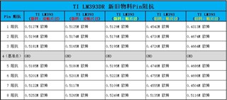
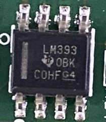
LM393DR PICTURE:
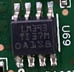
LM393DRG4 PICTURE:
  • Please show the schematic. What are the voltages at the two inputs?

  • Hello Zhang,

    There is a PCN to change the die of the LM393 family.

    The top picture datecode has the "new" die, and the lower picture has the "classic" die.

     See section 2.4 and 2.3 of the LM339 family appnote:

      Application Design Guidelines for LM339, LM393, TL331 Family Comparators

    Please ensure that the input voltages are at least 2V below the comparator supply voltage. As Clemens pointed out, please provide a schematic and/or measured voltages at the comparator pins for us to review.

    As the processes and devices are slightly different between the new and classic die, there will be slight differences in the pin to GND measurements. This is not a sign of failure.

  • Hi,

    Thanks for you kindly comment, and I don't search any different between LM393DR and LM393DRG4 for the electrical specifications in the PCB file,

    I know the "G4" is only environmental instructions by TI, we consider the LM393DR and LM393DRG4 are same electrical specifications, and we test in the same design, but LM393DRG4 is failure, the PIN to

    GND measurements is only the reference data to analyse this issue.

    I will send the schematic to your team when we go back to our office tomorrow, thanks.

  • Thanks Zhang, we will wait for your schematic. 

  • Hi,

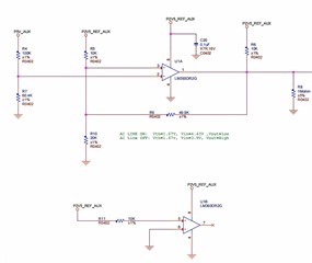
    Please refer to the schematic:

  • The LM393 is optimized for high supply voltages, up to 36 V. It needs a headroom of 2 V to the positive supply, so at lower supply voltages, the usable input voltage range becomes very small. At 2.5 V, the usable range is only from 0 V to 0.5 V.

    In your circuit, when one input is above 0.5 V, the electrical characteristics (especially propagation delay) are no longer guaranteed. When both inputs are above 0.5 V, the output is somewhat random and depends on the internal characteristics of the die. The change you are seeing is not related to "G4" or not, but to two different versions of the die.

    You need to use a comparator with rail-to-rail inputs, i.e., the LM393LV.

  • Hi Clemens,

    Thanks for your professional comment, so you mean, LM393DR also don't good for this design requirement, we need to use the rail-to-rail comparator like LM393LV and so on? thanks.

  • Hi Zhang,

    Yes, LM393LV is rail to rail and drop in replaceable so it can be able to handle input voltages up to the rail and has no limits on the input range. The output will be correct. 

  • Hello Zhang,

    As Clemens said, the LM393 is actually designed for higher voltages.  Running the LM393 at 2.5V is "running on fumes". The valid input range is only 0 to 500mV.

    They were lucky that the logic worked out with the older die. They were operating on the edge and I can almost guarantee them that it WILL fail at lower temperatures. Please see section 2.7 and 2.8 of the appnote that explains this in detail.

    We would recommend the LM393LV which could drop-in replace the LM393, or, change the resistor values to bring the thresholds below 500mV.

    The only difference between the LM393DR and LM393DRG4 is that the LM393DRG4 ensures you that you get only NiPdAu lead plating.

    Ordering the "generic" LM393DR, the plating can be either NiPdAu or Sn (tin), depending on where it was assembled.

    Either one could have either die at this time.

  • Hi Chi/ Paul,

    Thanks, this is a very bad news, because we have already got about 5Kpcs LM393DR on last two month, and we have no idea how to deal with these IC, 

    and please advise if there are any improve for schematic that we can use the LM393DR this time, thanks.

  • As Paul said, you can move the input voltages to below 0.5 V.

    In the current circuit, R5 and R10 generate a reference voltage of about 1.67 V. R4 and R7 divide an input of 4.43 V down to this voltage.

    For example, if you change to R5 = 25.5 kΩ and R10 = 4.7 kΩ, then you have a reference voltage of 0.461 V, and can use R4 = 118 kΩ, R7 = 13.7 kΩ.

  • Thanks Clemens for your continued excellent support of the forum.

    Zhang, Thanks for posting this on the forum.  It is unfortunate that this has occurred.  Maybe if there is material that you have not opened, you can return the material and purchase the LM393LV instead as this would remove the need to change the values and is really a better solution for low voltage applications.  The LM393 can be used in lower voltage applications but it forces one to keep the inputs in the proper common mode range as everyone is eluding to.  I am sorry you have found yourself in this position, but I believe my colleagues have provided the proper guidance to move forward.

    Chuck

  • Hi TI teams,

    Many thanks for your kindly support, we need to discuss this issue internal, your suggestion is very useful to us, thank you very much again.