Other Parts Discussed in Thread: LM339,
Hi,
We use the LM393 for the design, and the original designas is LM393DRG4, as we know, LM393DR is P2P to LM393DRG4, but the LM393DR has no output signal when we change the LM393DRG4 to LM393DR, please advise how to solve this iseu, thanks.
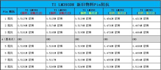
The PIN TO GND impedance testing report as below:
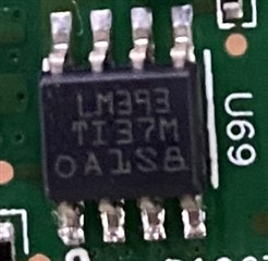
LM393DR PICTURE:
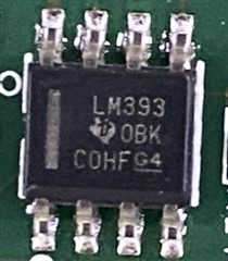
LM393DRG4 PICTURE: