This thread has been locked.

If you have a related question, please click the "Ask a related question" button in the top right corner. The newly created question will be automatically linked to this question.

OPA4990: OPA4990S control mode

Part Number: OPA4990
Other Parts Discussed in Thread: DAC70502

Hi team,

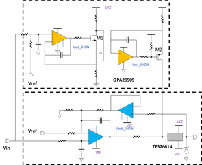
Currently I want to provide a discrete solution for customers which use DAC70502+OPA2990S/4990S to output both V/I on the same board.

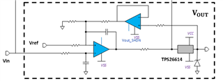
Our AE recommend this circuit for me as below but I want to ask you some questions:

1) Could you kindly help me understand the principle of the voltage output part? How to achieve output +-10V using two op amps?

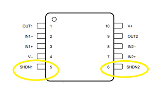
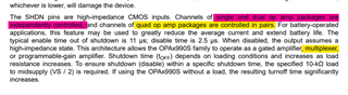
2) From datasheet, OPA4990S has a shutdown function so it can replace a multiplexer. But it did not specify which two channels are controlled at the same time. So I want to confirm that.


I also attached the one page introduction of this discrete solution for your reference. 

ISFA-426_VI_AOUT_onepager.pptx

Many thanks! 

Regards,

Maggie

  • Hey Maggie, 

    1. Your output voltage swing must be within the limits of the headroom from the +-supply rails. The headroom could be mV to a volt from each supply rail where distortion/clipping of the output signal could occur. The datasheet has provided different headroom specs with different loads and supply voltages:                                                                                                


    For your use case of +-10V output voltage and based off the datasheet, you can accommodate a headroom 200mV-300mV on a 2k load, essentially making your supply rails +-10.3V. To allow enough headroom between the output swing and supply rails,+-12V would be sufficient to avoid clipping your signal.   

    2. After reviewing your layout in your .pptx, it seems you are using a package with dual op-amps and the shutdown pins on the dual are independently controlled. 

    Regards,

    Ore. 

    TI is not responsible for any information outside the scope of this datasheet.   

  • Hey Maggie, 

    Ore is correct.

    If you need further explanation of how the circuit works I would leverage the following circuit design: https://www.ti.com/tool/CIRCUIT060014

    It can be used as a multiplexer with a not gate, an enable signal can be connected to one SHDN pin and a NOT on the other shutdown pin. 

    All the best,
    Caro 

  • Hi Ore,

    Thank you for your reply!

    I want to ask that what are the functions of the two op amps used for voltage output? The second op amp follow the VOUT and what's the function of the first op amp? I don't quite understand the principle of this part. Could you kindly so some explaination?

    Many thanks!

    Regards,

    Maggie

  • Hi Caro,

    Thank you so much for your help~

    Regards,

    Maggie

  • Hey Maggie,

    Regarding the op-amp at the bottom of the image, there's a voltage difference between Vref and Vin that gets amplified at the output terminal (vout_shdn). In its feedback path, there's a buffer that isolates all the impedances before it, allowing the output voltage from the current loop protector to be constant regardless of its impedance and the non-inverting input of the op-amp receives a constant voltage through the feedback path. The cap there is generally used to manipulate the bandwidth of the application. 

    Regards,

    Ore   

    Disclaimer: TI assumes no liability for applications assistance or customer product design. Customer is fully responsible for all design decisions. 

  • Hi Ore,

    Thank you so much for your quick reply! This really help me a lot!

    Regards,

    Maggie