


Hi,
I am a bit confused about the INA237AIDGSR IC ground and load ground relationship...
The datasheet mentions "the common-mode input range and device supply voltage are independent of each other" and the following diagram denotes the two grounds with different symbols:
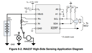
It is then stated that "The differential shunt voltage is measured between the IN+ and IN– pins, while the bus voltage is measured with respect to device ground."
May someone please explain me:
1) Can I expect any kind of isolation between the IC ground and the load ground in case I use only the IN+/IN- pins with a shunt, without connecting VBUS anywhere?
2) Can the VBUS be referenced to the load ground only and stay isolated from the IC power supply ground?
Thanks!
