This thread has been locked.

If you have a related question, please click the "Ask a related question" button in the top right corner. The newly created question will be automatically linked to this question.

VCA821:VCA821 emulation error

Part Number: VCA821
Other Parts Discussed in Thread: TINA-TI

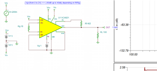
Hello I want to use VCA821 to design the input DC signal range in 0-1v or 0-2v Through the DAC input control chip pin Vg to achieve the output range of 0-3.3V, VCA chip power supply ± 5v Look at the data sheet, showing the input range ±Vs, but I downloaded the Tina simulation model on the official website SBOM366.TSC for simulation testing, but modified the Rf to 402Ω Rg to 18Ω The test operation is as follows: (1) The fixed Vg is 0.45V Input 1V output is 67.17mv, input 100mv output is 47mv (2) fixed Vg is 1V input 0.1V, output is 1.72V, input 0.2V, output 1.84, Vout/Vin ratio amplification is inconsistent, I don't know what the reason is.

I don't know if you can help modify the peripheral configuration circuit in the case of the simulation model on the official website, so as to realize the input DC range of VCA821 0-1v or 0-2v, and adjust the Vg to make its output range 0-3.3V

  • Hello cpin,

    Please see the two attached TINA-TI circuits:

    0_1VDC_vca821.TSC

    0_2VDC_vca821.TSC

    The test values for Rf = 402 are not for large input voltages or output swing ranges that are positive only.  Increasing Rf is required to swing to a higher positive voltage, such as 3.3V output.  Please try and edit the circuits I shared to address your application needs.

    Best,

    Alec

  • Hello Alec Saebeler   

      Thank you for your reply and help, I still have two questions here, the input range wants to make it 0-2v, do you need to change anything, you give here, it seems that the maximum input is only about 0.4v, when Vg is 2, the output is 3.01V, what is the functional relationship between Vg and G, how do I know how much G is after I change Vg, can the range of Vg only be from 0 to 2V, I have troubled you, best wishes

  • Hello cpin,

    Both circuits I sent you are set up to have a 0-3.3V output.  One circuit has a 1V amplitude square wave with a DC offset of 1V (shows 0-2V input case), the other circuit has a 0.5V amplitude square wave input with a DC offset of 0.5V (shows 0-1V input case).

    The maximum gain is set by Rf & Rg.  The Vg pin is used to vary the gain down (decrease) 40dB from the maximum gain.  Setting Vg to 2V will operate the VCA821 at maximum gain (Rf + Rg), while setting Vg = 0V will operate the VCA821 at the lowest possible gain (40dB from max gain).

    The VCA821 is continuously variable, which indicates there are no discrete gain steps, but gain accuracy to ±0.3 dB.

    Best,

    Alec