This thread has been locked.

If you have a related question, please click the "Ask a related question" button in the top right corner. The newly created question will be automatically linked to this question.

INA240: Inquiry on INA240A2PWR Output Peaks Duration

Part Number: INA240
Other Parts Discussed in Thread: INA241A,

Dear Texas Instruments Customer Service,

I hope this message finds you well. I am reaching out to seek some clarification regarding an observation I have made with the INA240A2PWR current-sense amplifier in our recent project implementation.

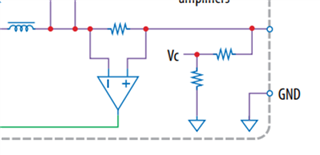
We have set up the INA240A2PWR in our circuit as per the application schematic provided in the datasheet. In our oscilloscope measurements, the green and yellow traces represent the potentials before and after the shunt resistor, respectively, and the purple trace is the differential signal. The output from the INA240A2PWR is displayed in pink/red. 


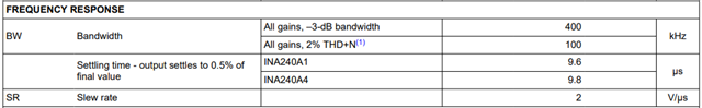
While reviewing the output, I noticed that the peaks at the INA240A2PWR's output exhibit a duration that is an order of magnitude larger than the typical response shown in the datasheet. Specifically, the peaks in the datasheet appear to be around 1 µs, whereas in our measurements, they are about 10 µs.


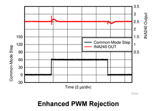
Could this discrepancy in peak duration be attributed to the PWM rejection capability of the device, or might there be another factor at play here? Any insights you could provide on whether this behavior is expected, or if it indicates a potential issue, would be greatly appreciated.

I am implementing field-oriented control using the circuit and an STM32G4 microcontroller. I have noticed that at switching frequencies above 25 kHz, the current measurement starts to become increasingly noisy. The rapid switching causes an overlay of peaks at the output of the INAs.


Inline current sensing:

INA240A2PWR:

CircuitDiagramINA240A2

Before the SHUNT is an EMI-Filter:

  • The INA241A/B datasheet says:

    When INA241x senses the large common-mode ΔV/Δt transients, it holds the output for 1 μs, thereby preventing the common-mode disturbance from propagating to the output. If another common-mode transient occurs during the following 3 μs, INA241x relies on high BW and AC CMMR to attenuate the effect of common-mode transient. The enhanced PWM rejection is achieved up to a PWM frequency of 125 kHz or if common-mode transient edges are separated by a 3 μs interval or more.

    I do not know if or how the INA240's PWM rejection is different.

  • Thank you, Clemens, for your help. I applied a supply voltage of 36 volts. In the datasheet of the INA240, I found something about the Slew Rate (2 V/µs) and Setting time. "Settling time - output settles to 0.5% of final value".

    I don't quite understand what these 2 specifications tell me. So, do I have a percentage deviation of 0.5% from my final value after 9.6 µs? The Slew Rate in electrical components is a measure of how quickly the output voltage of the component can respond to changes in the input signal. As can be seen in the oscilloscope image, the jump of both input signals (green and yellow) goes from 0 V to 36 V. Can the phase shift then be approximately calculated with ~36 V / (2 V/µs)? I could take new measurements next week with a different supply voltage and observe that.

    The datasheet shows a diagram (see above) with a step(black) from 0 to 60 volts where the outputpeak (red) is just 1 µs long. This doesn't match up with the stated 9.6 µs nor with the 60V/(2 V/µs).

  • These specifications describe the step response; see figure 7-20.

    Anyway, the INA240 is designed to be resistant to common-mode noise. But the red trace shows differential noise, which is considered part of the signal and will not be suppressed. And some of the peaks happen before the falling edge on the yellow/green traces, so are not directly caused by it.

    Please show the board layout. Are there any digital signals near the current sense traces?

  • Near the INAs, there are no digital signals. Two INAs have PWM signals passing by, and I measured at the INA that is furthest away from them. I think this is due to the measurement method. When I only measured the green signal, these interferences were less present. Im using the EPC9146 Board- the gerber files are online available. 

    What are possible reasons for the peak being much longer than indicated in the datasheet? Could the resistors, capacitors, etc., have been chosen incorrectly?

  • Hi Daniel,

    The datasheet curve is showing the common mode disturbance only after a common mode transition, which lasts between 1 to 2 uS.

    It appear to me the over shoots in your scope pictures have a large portion due to differential input. If there is a way not running any current through the shunt resistors, while only toggling the common mode, you should see similar common mode response.

    Regards, Guang  

  • Hello Guang,
    Thank you for your response. However, I am having trouble replicating that behavior exactly. Could you please clarify what is meant by "Setting Time" as mentioned in the datasheet? Today, I conducted new tests without connecting the motor windings, ensuring that no current passes through the shunt. Additionally, I modified my code so that only one gate opens instead of all three.

    The test shows that the height of the current peak depends on the applied voltage, but the time delay remains nearly the same. The measured setting time is consistently 9.6 µs or close to this, as specified in the datasheet (which is already attached above in the chat).

    Green: Step 
    Pink: Phase 3
    Yellow: Phase 2

    Since Phase 2 and Phase 3 are connected to the same ground, Phase 2 also detects the gate switches.


    35 V Voltage:

    25V Voltage:

  • Hi Daniel,

    The 9.6uS is regarding differential input step settling, with constant common mode voltage.

    In your circuit, do you have any input/output filtering around the INA? If so, can you depopulate them and repeat the common mode test? The common mode should settle in 2uS, not 10uS.

    Regards, Guang  

  • Hi Guang,
    I checked the datasheet for my evaluation board once more and saw that the path has two resistors connecting it to ground (attached picture). This means there’s always some current in the shunt. So, my last tests weren't done with common mode. I need to remove one resistor. But I'll stop there. I’ve learned what I needed about how the datasheet's information is different from what I have. When the system is running, the peak length always matches the 9.6 µs settling time mentioned, because it's not operating in the common mode. In summary, I can't just keep increasing the PWM frequency of my gates, because I keep measuring at that peak. 
    This is what the green signals on the oscilloscope images above are showing, where i compared 12,5 kHz with 100 kHz PWM.

    Thank you Guang!!   

  • Hi Daniel,

    You’re exactly correct that the PWM frequency can’t keep increasing, eventually the settling imposes a limit on the switching frequency and duty cycle.

    I’m glad it is clear now, please let us know if we can be of any assistance in the future

    Regards, Guang