This thread has been locked.

If you have a related question, please click the "Ask a related question" button in the top right corner. The newly created question will be automatically linked to this question.

LM324B: Low-side current sense gain

Part Number: LM324B

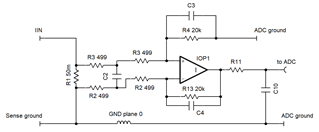
I am trying to do a low-side current sense circuit.  I basically copied a circuit from SBOA190–March 2017.  Using the gain formula, I tried for a gain of 20.  The problem is, I am seem to be getting a gain of 1.  I have double checked the component values and just about everything else I can think of.  I don't see why I am getting unity gain instead of a gain of 20.  Any insights would be appreciated. 

 QCM RevX Schematic_cropped.pdf

  • What are the voltages that you measure at the top of the shunt resistor, at both input pins, and at the output?

  • Robert,

    Gain is (VOUT2 - VOUT1) / (VIN2 - VIN1); two points are needed. You can expect an output offset error of (20+1)*Vos (Vos is op amp input offset error)

  • Thanks for the reply.  I am using an electronic load made by an English firm named TTi, an LD300, to put a constant 1A load on this circuit.  I measured .054V at the top of the sense resistor, .051 at the positive input, .053 at the negative input and .052 at the output.  I should mention that I know just enough analog to be dangerous, I am mostly a digital engineer and programmer.  Not sure if these values make sense.  

  • Sorry but I am not sure what Vouts you are referring to.  If you look at my circuit I copied from the TI app note mentioned this is measuring low side current with one side of the current sense resistor grounded, so I assume on of your Vins is ground. As I increase the load from 0 to 4A I get 0V to .2V at the op-amp output. 

  • Robert,

    54mV at sense and 51mV at non-inverting op amp input makes sense.

    53mV at inverting input also make sense; that is close to noninverting input voltage.

    52mV at output doesn't make sense. 

    Here are some reasons why that could happen.

    R2 is very high (>100k), missing, open solder joint

    R2 GND is open or near 50mV

    R13 is very low <100 ohms 

  • Hi, I have built 3 boards, all with the same results.  My PCB software has a very good DRC so I know the PCB is correct.  I also have all boards tested at the manufacturer to ensure compliance.  The PCB is a 4-layer board with a solid ground plane.  I have actually measured the resistors before mounting them.  I build the last board with only one channel stuffed and nothing else on the board.  I will check the nodes you mention but I do believe all the solder joints are good (based on 3 boards acting identical).  This is such a simple circuit I am baffled where I could have gone wrong.  I will get back with my results on the nodes you mention. 

  • Hi, don't know if this helps at all but here is pdf of the layout.

    Multilayer Composite Print.pdf

    Thanks

  • Hi, well, on the 3rd board I did have a bad solder joint on R2.  Don't know how I missed that, I thought I was especially careful on the 3rd, partially populated board.  Strange thing was, it was on the trace going to the op-amp-, not ground.  When I fixed that I got 1.010V at the output.  

    If you have time, I could use some advice on filtering.  I am measuring current of "digital" servos that pulse their motors at about 400Hz. What you see on the scope is a peak current draw, up to 4A for somewhere between 0 and 2.0ms with 0A for the rest of the time before the next pulse.  I put a filter on the output of the op-amp before the A/D but am not sure that is the best way.  Can you give me some insight? Thanks, 

  • Robert,

    It appears to me that R2 and R4 (see blue boxes) have one small easy to solder pad on one side. The other side has a large pad that is heat sinking making it hard to solder. R3 (green box) look OK 

  • True, but amazingly that was not where the bad solder joint was.  It was the other side of R2. Now I just have to figure out why my other boards have issues.  I am usually good at soldering and checking.  Guess I was in a rush.  Dumb.  

  • Robert,

    Use as many of these as you like 

    R4 should terminate at the ADC ground point, not sense resistor ground point. ADC ground is slightly better than other points on ground plane. 

    (R2+R3) & C2 is the 1st low pass filter.

    C3=C4 and R4=R13 are second low pass.

    R11 and C10 are the last low pass filter. 

  • Thank you.  I will change R4's location on the next layout.  I will also incorporate some of these into my next layout and experiment with them.  I appreciate you taking the time to answer this question.  Bob