This thread has been locked.

If you have a related question, please click the "Ask a related question" button in the top right corner. The newly created question will be automatically linked to this question.

OPA380: Amplifiers forum

Part Number: OPA380
Other Parts Discussed in Thread: OPA830

Hello,

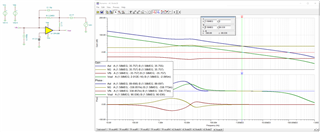
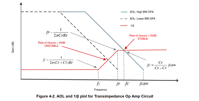
I am currently doing an project with transimpedance amplifier for a photodioe, and I would like to test their stability. From some websites, I got an idea that I can verify this through plotting the curve for Aol and 1⁄β, just like shown in the figure. If the rate of closure between Aol and 1⁄β is equal to 20dB, the system is stable.


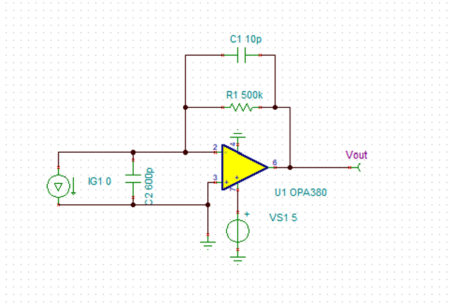
However, I tried to plot them and the result is not very correct, the schematic for test and results is shown as follow:

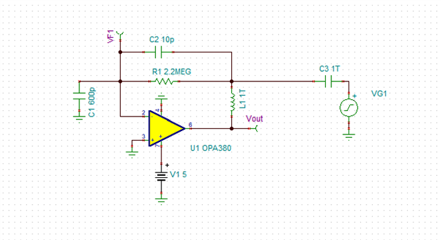
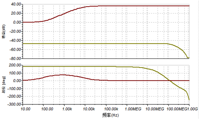
The curve equation is :

Aol=Vout(s)/VF1(s)

Noise=1//VF1(s)

How can I modify the simulation to get the correct result?

Best wishes,

Kiwiki

  • Hi Kiwiki,

    I believe the reason you are not getting good results has to do with the noninverting terminal of the OPA830 being tied to GND in your simulation. When you are operating the op amp at single supply, the noninverting terminal needs to have a bias voltage, otherwise output swing rails will be met which affects the device performance. Setting the voltage bias to midsupply (2.5V) I get the following results:

    There are actually a couple ways to determine the stability of the circuit: as you mentioned you can determine the point where the Aol and noise gain curves cross and measure the phase of Aol*B (or Vout) at that frequency. You can also measure the 0dB point of Vout and then measure the phase of Vout at this frequency. The phase of Vout would be the phase margin of the system; for stability, it is recommended to have a phase margin of 45 degrees or greater. You can also look at rate of closure using the method you indicated above.

    Thanks,

    Nick

  • Hi Nick,

    Thanks a lot for your answer, I really forgot this points. After testing, I can get the correct result. 

    However, Can I just have a check of two points you mentioned?

    Regarding the  bias of the non-inverting input, I want to make photodiode working under no bias situation, which is the photovoltaic mode, that is why I connect both inputs to zero, the schematics for the whole TIA circuit is shown as here. The amplification results for the circuit is correct. Therefore, do I still need to bias the non-inverting input?

    Another question is for th phase margin. As the results for PM is about 90 degree, if it is supposed to reduce a little bit since it is far more larger than 45 degree.

    Thanks again for all of your help.

    Best wishes,

    Kiwiki

  • Hi Kiwiki,

    Thank you for clarifying your application. To have your photodiode operating in photovoltaic mode, you will need the IN+ pin to be biased at 0V with the photodiode biased at 0V as well. Because of this, it is best to operate the TIA with split supplies (+/-2.5V) or with some negative voltage so that the output voltage swing limits goes below 0V.

    Regarding your question about phase margin: the simulation results were a representation of ideal conditions and did not factor in any parasitics from your layout. The parasitics will likely decrease your phase margin below 90 degrees some. Even still, it is not of huge concern to have a phase margin this large.

    Thanks,

    Nick

  • Hi Nick,

    Thanks for your reply! It is really helpful.

    Best wishes,

    Kiwiki

  • Hi Nick,

    Sorry to bother you again. Could I ask a further question?

    Why the noise gain would not start at 0dB, but with a positive value? I have tested for several time, and I found this start value would increase when I increase my feedback resistor. Is this the problem of my feedback resistor?

    Best wishes,

    Kiwiki

  • Hi Kiwiki,

    Please allow me a few days to get back to you with an answer to this. In the meantime, can you attach your simulation file so that I can ensure I am testing the same configuration that you are and that the values I see align with simulation values you are obtaining?

    Thanks,

    Nick

  • Hi Nick,

    Thanks a lot! Sure, the file is attached as follow:

    OPA380.TSC

    What I am confused is that it will have a positive gain at the low frequency range and it seems to have another pole and zero after the pole brought from the addition of feedback capacitor. I don't know where are they from.

    If you have any suggestion, please let me know.

    Best wishes,

    Kiwiki

  • Hi Kiwiki,

    Thank you for providing the file. I will get back to you with an answer on Monday due to the US holiday. I checking into if this is just the model behavior.

    Thanks,

    Nick

  • Hi Nick,

    Of course. Thank you very much for your kind reply. I sincerely appreciate your help. 

    Best wishes,

    Kiwiki

  • Hi Kiwiki,

    The noise gain at low frequency ranges will not necessarily be 0dB. It is dictated by Rf and Rg values (NG at low frequency = 20*log[1+Rf/Rg]). 

    I suspect that the input common mode resistance and Rf is what is causing the NG above 0dB. You will notice that lowering the Rf will decrease the NG.

    Thanks,

    Nick