LMP7718: Max possible gain for a 100khz sinewave input ?

Part Number: LMP7718
Other Parts Discussed in Thread: THS4032

Hi There,

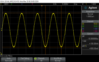
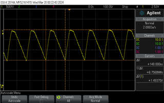
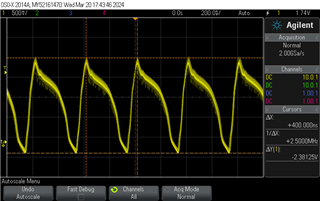
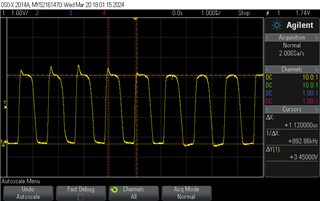
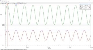
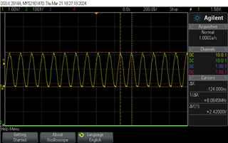
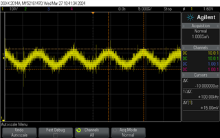
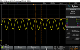
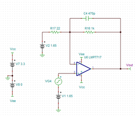
I am trying to amplify a sine wave signal of order of 40mv peak to peak. The signal oscillates from 1.57V to 1.61V so its not at absolute zero potential when going down. The gain is set to 46 as per circuit. The circuit used to work with LT6231IS8#PBF but upon changing to LMP7718MAE/NOPB the output is not as expected. It should be a 600mV peak to peak signal instead I am getting triangle wave of 6 MHz. 

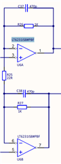
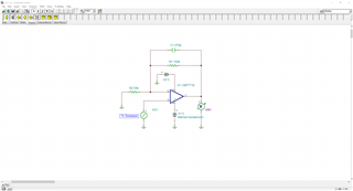
Please see attached circuit snap for your kind reference. I feel that Gain is set beyond the IC limit, please let me know.

Thanks..!!!


  • Hi Ishan,

    The gain configuration should not be a huge problem other than a more limited bandwidth which should be fine in the configuration you're in and the 100kHz limit you require. I was wondering if you remove the capacitor at the feedback network what impact if any it has on the response. I was also curious if you could provide the supplies of the LMP7718. Is the difference amplifier the same for the LT6231 and the LMP7718?

    Best Regards,

    Ignacio

  • Hi Ignacio,

    I removed the capacitors C37 and C38 as per your suggestion, the frequency of the output is now reduced to 2.5MHz instead of 6.75MHz previously with capacitors. Please see attached image for your kind reference.

    The supply is coming from a linear regulator at 3.3VDC, its a single supply. Both LT6231 and LMP7718 are pin compatible so everything remains same on PCB.

    I feel that resistor values are too small, I can replace 1k with 10k and 22r with 220 ohm and check. Will update you with the waveforms.

  • Hi Ignacio,

    I replaced feedback resistors with 100k instead of 1k and 220R instead of 22R, the gain is same just resistor values are increased. With this settings, the frequency of output signal is now 892KHz and it seems that OPAM is saturating as the amplitude is 3.3V. Please see attached image for your kind reference. 

    Please let me know your thoughts on same. I will try some other iterations and update you if needed.

    Thanks..!!!

  • Hi Ignacio,

    I tried with different gain settings by changing value of R25 but no luck, even at unity gain it outputs same signal as uploaded above. Then I simulated a non-inverting amplifier in TINA TI. the gain settings doesn't seem to work, thought the output frequency matches the input. Please see attached images for your kind reference.

    Thanks..!!!

  • Hi Ishan,

    The device will not work in this low of a gain as it is decompensated and requires a minimum gain of 10V/V, which in the normal configuration of ~46V/V meets this requirement. As far as the 100k Rf resistor, we do not recommend a value this high as it starts to affect other aspects of the design, we recommend a value close to the datasheet. In this case 1k to 10k is a good range for this device. I was curious if there was a way to check the inputs of the devices and make sure we aren't violating any common-mode input range conditions since it is configured with a single supply. Is there also a way to disconnect anything at the output of the LMP7718, so removing the difference amplifier stage and probing directly at the output of the channels. This will help isolate the LMP7718 and remove other potential factors.

    Best Regards,

    Ignacio

  • Hi Ignacio,

    Thanks for the kind response..!!!

    I got your point. I will keep the resistor values as per your datasheet guidelines.

    Regarding the inputs, it seems as if input is affected due to feedback in OPAM. Input signal is not same as it is in original design. I will share a snap of inputs shortly. 

    I can easily isolate the output pins as I have a 10R at the output. The opam output goes into a differential ADC via an RC filter.

    I also did a small iteration where I placed the chip on a bare pcb and made the voltage follower circuit with 1k feedback resistor. The input was a 1V DC signal but output is an 8MHz sinewave with 2.42V amplitude, attached is the signal for your kind reference.

    Thanks..!!!

  • Hi Ishan,

    That is a good point, in general what is the input signal you are applying? Is it biased appropriately to account for the single supply configuration? If it is easier, could you share a tina circuit to show exactly how it is configured and what the input signal is supposed to be along with any biases you have for the circuit. As for the small iteration, this is expected behavior since the amplifier is decompensated which requires a minimum gain of 10V/V. Therefore 1V/V will definitely result in instability and give erroneous results. Would you be able to try the same unit with the gain you were implementing previously of ~46V/V. In this higher gain configuration if you can also ensure nothing is connected to the output of the device as well.

    Best Regards,

    Ignacio

  • Hi Ignacio,

    Let me explain over all circuit. The signal originates from a digital synthesizer chip (500mV/100khz pk-pk), which is then amplified by OPAM to 8V pk-pk, this signal goes into on board PCB coils and from the coils it goes again into LMP7718. When the signal exits coils it is 40mV pk-pk, the application is ferrous material detection. Please note that as we have used single supply opams, all the signals are having zero shifted to 1.6V.

    I tried the off board chip with a gain of 46V, just as in original circuit and it works fine. It seems the issue us with the on board input signal and compatibility. I guess this may be due to 1.6V reference level, but I am not sure. I have ordered one more chip from a different manufacturer and will also check it.

    Thanks..!!!

  • Hi Ishan,

    Thank you for the explanation of your circuit. That is good that the circuit is working as expected in that gain. I was wondering, when you put the single amplifier in a gain of 46V/V, what values for the feedback network did you use? I was also wondering what input signal you used to validate that the circuit worked appropriately, was it a basic signal from a function generator with an offset of 1.6V or the actual signal outputted from the coils?

    Best Regards,

    Ignacio 

  • Hi Ignacio,

    I used the same resistor network of 1k and 22R as in original circuit. I used a 100mV DC signal from a bench-top power supply as an input. I wanted to use actual signal but I can't because there is an onboard potentiometer and ADC involved that measures the output and provides input signal accordingly.

    But it is very clear that the chip is not compatible with my circuit as it is otherwise it would have worked straight away. I am still unsure about why its not working.

    Thanks..!!!

  • Hi Ishan,

    Our tool cross reference tool suggests the THS4032 as a potential replacement for the LT device, however the minimum supply requirement is 9V. In simulation, the device does not suggest any potential failure points and certainly does not show the signal you are measuring. Is there a way you could measure the input signal with the LT device, just so we can see exactly what is going into the device.

    Best Regards,

    Ignacio 

  • Hi Ignacio,

    Thanks for suggesting alternate part, it has a different footprint and supply requirements than present one, so I won't be able to use it. Please let me know if there is any drop and replace part available. 

    Please see attached input signal and output signals at the LT device. The input is a 15mv pk-pk 100khz sinewave, with reference at 1.6V while output is a 1.1V pk-pk 100khz sinewave.

    Please note that these are standby signals, when I insert the ferrous material in the coils these waveforms will increase in amplitude.

    Thanks..!!!

  • Hi Ignacio,

    I did one last iteration with a function generator, the chip works fine with analog sinewave input referenced to 0V (i.e. oscillating above and below 0V) but it doesn't work with analog offset input signals that is signal oscillating above and below a non-zero voltage level. The output starts degrading as soon as I start to increase the offset by couple of milli-volts and then it saturates to supply voltage once the offset voltage is around 200mV. The gain setup in this iteration is 46 using 1k and 22R.

    Thanks..!!!

  • Hi Ishan,

    Was the design configured in this way with the Rg resistor also biased as you shifted from 0V offset to 1.65V? Having an appropriate offset to correctly bias the input of a single supply opamp should not result in any problems.

    Best Regards,

    Ignacio

  • Hi Ignacio,

    Sorry for the delayed response..!!!

    Yes, the design was configured same on PCB and also on the stand alone PCB. 

    Regards..!!!

  • Hi Ishan,

    If the circuit is biased similar to the design above, then having an offset shift should not be a problem. Could you send a schematic of the stand alone PCB where you saw the device saturate when increasing the offset to 200mV. With an offset of 0V did you start with a split supply? 

    Best Regards,

    Ignacio

  • Hi Ignacio,

    I used an old PCB with some minor modifications to check the chip standalone. Please see attached image for your kind reference. I didn't used a split supply, it was a normal 3.3V setting just as in the design of my PCB.

  • Hi Ishan,

    Assuming the gain resistor is R8, is this voltage on the left pad grounded or at 1.65? I am trying to understand why any sort of offset is causing the device to saturate.

    Best Regards,

    Ignacio

  • Hi Ignacio,

    Yes you are correct, the left pad is Grounded. This is also surprising to me so I ordered one more chip, this time from Analog Devices and from same series, LT1807CS8 and this is also misbehaving. But the LT6231 works perfectly OK and while I was double checking the datasheet of LT6231 it has 50uV of offset, I guess it is perfectly fine and there is not much room for improvement in terms of component accuracy. But if TI chip works then it would be half the price of current part and that would be very desirable.

    Thanks..!!!

  • Hi Ishan,

    Thank you for clarifying, that should be where the saturation issue is coming from when testing the device and changing the offset. The left pad should be set to mid-supply (1.65V) when inputting a signal with the same offset of 1.65V. This was the idea I was trying to highlight in the image I shared previously if you are trying to test the device as a single amplifier when debugging. As you can see the left side of R17 is not grounded, instead set to mid supply. This will allow your input to have an offset and not completely saturate like you were originally seeing.

    Best Regards,

    Ignacio