A related question is a question created from another question. When the related question is created, it will be automatically linked to the original question.
If you have a related question, please click the "Ask a related question" button in the top right corner. The newly created question will be automatically linked to this question.
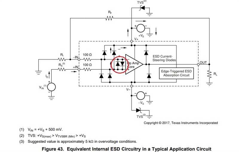
OPA4202 is a bipolar input quad amplifier with back-to-back input protection diodes between the input terminals - see below.
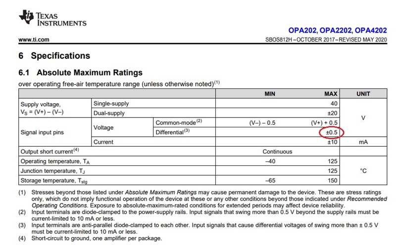
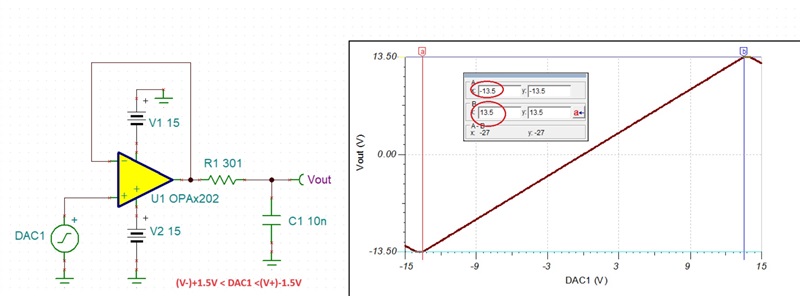
For this reason, it is NOT well-suited for the comparator application you seem to try to implement in your schematic. Since its absolute maximum differential voltage is limited to just +/-0.5V, using it as comparator may result in erroneous voltage tripping point - see below.
If you need further assistance, please provide basic information like what is it exactly that you try to do? Also, please provide information about voltage supplies and the range of the input voltages applied to the input of the amplifier. Btw, what sort of Tina simulation are you asking for? AC, DC, transient, etc.?
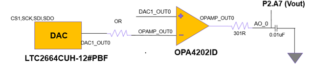
Currently in my schematic the unity gain OP-amp which is DNP (donot populate ) in my board. When it is in DNP, we need to place this 0R for connectivity to OPAMP_OUT0 then to 301R. When this OP-AMP is not DNP ( i.e. when it is populated in board ) , then the 0R resistor will be removed and DAC_OUT0 directly connected to OP-AMP's DAC_OUT0
Please provide information about voltage supplies and the range of the input voltages applied to the input of the amplifier. Btw, what sort of Tina simulation are you asking for? AC sweep, DC sweep or transient response, etc.?
For the alternative to DAC LTC2664CUH12-#PBF, you need to contact appropriate DCC-DAC product line. Just so you know, E2E is a support forum helping with design related problems and not a design house. You need to do diligence in your design efforts especially in case of very limited design description in line with "kindly provide the TINA simulation for the above circuit."