This thread has been locked.

If you have a related question, please click the "Ask a related question" button in the top right corner. The newly created question will be automatically linked to this question.

OPA2374: Unexpected input coupling

Part Number: OPA2374
Other Parts Discussed in Thread: TLV9062, MCP6292, TSV912, TLV9152, OPA2323

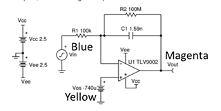
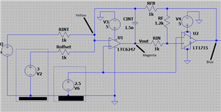
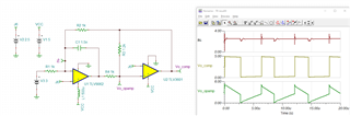
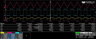
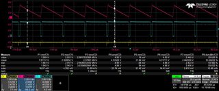
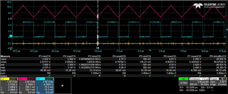
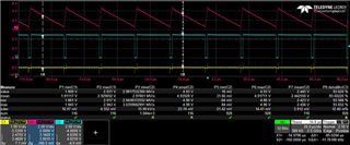
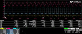
When testing this series of op-amp in an integrator circuit we discovered some significant coupling between the input and the output feedback.  This phenomenon was not experienced with other op amps of a different series (Notably the MCP6292IDDFR and TSV912AIDDFR).  It was also seen when using the TLV9152IDDFR and TLV9062IDDFR op amps within the same circuit.  The attached plots detail the problem further:

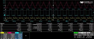
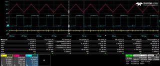
The inverting input is the yellow trace, output from the op-amp is in magenta, and the feedback is in blue. 

Any help in explaining or understanding why this event is happening and why it only occurs on some of these parts would be appreciated.

  • Hi Ryan, 

    Welcome to E2E!

    This is my interpretation of the schematic you may be using (supply voltage and components may vary): 

    Could you confirm if this is what your setup is and if not, please provide your schematic details? 

    Regards,
    Ashley

  • Hi Ashley,

    Here is an image of a spice model for the circuit with the signal measurement points labelled. (Note: some schematic notes were redacted but are not relevant)

  • Hey Ryan, 

    LTC6247 is an dual op amp and LT1715 is a dual comparator. 

    Is the OPA2374 used for both of these? 

    All the best,
    Caro

  • Hi Caro,

    No, The OPA2374 is used to replace just the LTC6247

    Best,

    Ryan Donoghue

  • Hi Ryan, 

    Thank you for the clarification. Did the comparator device and passives remain the same when the op amp was changed? 

    Could you clarify what the setup and behavior was for the other devices mentioned in the beginning of the post (MCP6292IDDFR, TSV912AIDDFR, TLV9152IDDFR and TLV9062IDDFR)? Which devices do the waveforms apply to? 

    Thank you!
    Best Regards,
    Ashley

  • Hi Ashley,

    I can confirm all other components remained the same when the op amp was changed.

    The setup for all devices was the same, these were used as drop-in replacements on a PCB and jumper wire was used to observe the signals with an oscilloscope for verification. MCP6292IDDFR & TSV912AIDDFR had waveforms similar to the baseline image provided (The yellow trace being just a DC voltage).  The other op amps all exhibited some kind of distortion on the yellow trace similar to the OPA2374 that seemed to align with the blue waveform.

    Best,

    Ryan Donoghue

  • Hi Ryan, 

    Thanks for the confirmation on the different devices you've tested. I noticed the spice model schematic do not include any decoupling capacitors on the supply. Are these implemented in the PCB design? 

    Regards,
    Ashley

  • Yes, decoupling caps are used in the final design

  • Hi Ryan, 

    What value capacitors are you using and how far from the devices they placed on the PCB? 

    Regards,
    Ashley

  • Hi Ashley,

    I'm not sure the capacitors are related to this issue since all devices used the same decoupling capacitors placed in the same locations.  Can you provide some justification as to why, for example, the MCP6292IDDFR would need different decoupling capacitors than the OPA2374?

    Note: the decoupling capacitors are shown to be sufficient in the final design with the original part.

    Best,

    Ryan Donoghue

  • Hi Ryan, 

    Understood that the decoupling capacitors haven't changed in the design. However, we are wanting more information to better understand your issue and we believe that the value or location of the decoupling capacitance may play a role in this. The MCP6292, TSV912, and TLV9062 are based on similar designs and should function similarly in the same application so we are exploring other possibilities that could factor into the different behaviors. 

    The scope captures provided show that the inputs are being pulled apart, which is indicative of some limitation of the op amp driving the feedback loop. This usually means the feedback loop either cannot supply sufficient voltage or current, or it cannot supply fast enough to equalize the voltage on the op amp inputs. The differential input voltage eventually recovers after it dips, so it appears the op amp cannot source current fast enough to equalize the inputs when the inputs are being pulled apart on the falling edge of the output comparator. 

    Please help to provide some more information on the decoupling capacitors so we can rule out and narrow down what could be causing the issue. 

    Thank you!
    Best Regards,
    Ashley

  • Hi Ashley,

    Understood.  The decoupling cap used on that part is a 100nF/10V capacitor.  Physically it is directly adjacent to the V- pin (pin 4) <45 mil apart. 

    I am unfortunately not able to share an image of the PCB or any diagrams as to placement beyond that.

    Best,

    Ryan Donoghue

  • Hi Ryan, 

    Thanks for the clarification. What about on the V+ (near pin 8) side? 

    Regards,
    Ashley

  • Hi Ryan, 

    I was testing your circuit in simulation and was able to mimic the behavior of the inputs being pulled apart by placing a 500uH inductor connected to the V+ pin. I understand that 500uH is a large inductance value to have from traces and normal parasitic behaviors but believe this illustrates what might be happening without a decoupling capacitor close enough to V+. 

    Regards,
    Ashley

  • Hi Ashley,

    Since the decoupling capacitor is used between the supply line the same cap is used for decoupling the V+ pin.  The trace length between these components is longer on the V+ pin (~604 mils) but I don't think that would create that high of an inductance.  Hope this clarifies some things.

    The behavior you're seeing in the simulation also doesn't seem to explain what we saw in our experimental results.  There is a distinct level shift in the DC voltage that can be seen on all the op-amps that corresponds to the high and low transitions in the blue waveform.  I've attached more photos to detail further:

    The Left image is taken from the TLV9152, and the second image is taken from TLV9062.  The deviations in the TLV9062 are slight however are still unexpected and undesirable for our application.

    Best,

    Ryan Donoghue

  • Hi Ryan, 

    Noted - thank you for the additional waveforms. It does seem there is slight deviation of behaviors among the different parts. 

    For the TLV9062, could you re-test this one and re-capture the waveform? It appears that the circuit was broken somehow and the integrator function was not working properly. 

    It appears that this may be an effect of the devices needing a larger input differential voltage in order for the op amp to behave fast enough. We may need to try a higher bandwidth and/or higher slew rate part to see if this improves the distortion. 

    I recommend testing our new OPA2323 device. This part has a higher bandwidth and slew rate than the parts tested earlier and may yield better results. 

    Please let me know if you have further questions.
    Thank you!

    Regards,
    Ashley

  • Hi Ashley,

    The output from the integrator (the magenta waveform) looks how we'd expect (with some error given the input waveform isn't what we expect), what makes you say the integrator is broken?

    Additionally, I wasn't aware the slew rate changed based on our input voltages.  We spec-ed the part base on the datasheets slew rate being more than sufficient, if that slew rate changes based on our inputs can you inform me on how to adjust the datasheet slew rate so we can reject non-viable parts before we test?

    Best,

    Ryan Donoghue

  • Hi Ryan, 

    Apologies, I believe I have misunderstood what is considered the "good" or "desirable" behavior for this application and what is the "abnormal" behavior. I have attached a powerpoint slide that consolidates all the scope shots you provided and labeled what my understanding is after your last post. Please help to clarify what error you are trying to remove. Is the focus on the inputs to remove the distortion? Or the frequency or shape of the integrator waveform? 

    Integrator_circuit_e2e.pptx

    What slew rate spec were you basing the application on? Slew rate is a output rate of change for a large input signal, so for some devices that have slew boost, a small input differential voltage will not be enough for the expected slew rate behavior. We have an application note with more information on slew rate here: https://www.ti.com/lit/pdf/sloa332

    This is why we are recommending testing the OPA2323 to see if this will help to solve this issues seen in the application. If you need assistance with this, please let us know. 

    Regards,
    Ashley

  • Hi Ashley,

    I understand now, thank you.  Yes, you are right that there is distortion on the integrator output, I attributed this distortion to the inputs being "pulled apart".  As such, our focus has been trying to understand why the inverting input is being affected and why it seems to correlate with the blue waveform.  Any ideas as to why that might be occurring would be great.

    The unknown device listed in the PowerPoint you shared is our baseline (the part currently on the board).  It is the same part number as what's on the simulation, the LTC6247.  We are aiming for a slew rate above 3V/uS.

    We will look into the OPA2323, thank you for the suggestion.

    Best,

    Ryan Donoghue

  • Hi Ryan, 

    So between the LTC6247 and TLV9062 behavior, which one is the desired waveform from a output (both integrator and comparator side)? There seems to be a difference from a time scale too. 

    LTC6247:

    TLV9062: 

    Thank you!
    Best Regards,
    Ashley

  • Hi Ashley,

    The LTC6247 is the desired behavior.  I realize these images are at two different differential voltages, so I have attached the same plots at the same voltage.

    On the left is the LTC6247 (our baseline) and on the right is the TLV9062.  Hope this helps.

    Best regards,

    Ryan Donoghue

  • Hi Ryan, 

    Understood, thanks for the new images and clarifying the baseline behavior. 

    The "inputs pulling apart" behavior is due to the output voltage not changing fast enough with the small input difference. This distortion effect is likely then impacting the comparator output. To get a lower distortion signal, you would need a device that has a high bandwidth and high natural slew rate. This was why we recommended the OPA2323 as this device has a high natural slew rate. 

    Regards,
    Ashley