A related question is a question created from another question. When the related question is created, it will be automatically linked to the original question.
If you have a related question, please click the "Ask a related question" button in the top right corner. The newly created question will be automatically linked to this question.
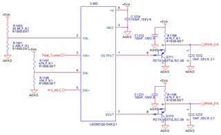
Currently, your 1IN- voltage is 0.496V and your 2IN- voltage is 1.210V. This means that Output will pull low whenever Total_Current is < 0.496V and high whenever Total_Current is >0.496V. 2OUT will pull low whenever HV_ADC is < 1.210V and high whenever HV_ADC is >1.210V.
The LM2903-Q1 has an input common mode voltage requirement of V- to VCC - 2V over temperature; this means that you will need to keep your input voltages within that range to ensure proper operation of the comparator. Both IN- are within the range, but you need to ensure that Total_Current and HV_ADC are also within the range.
The pre-biased PNP seems pretty redundant to me; is there a specific reason why you selected to have them in the design? If the output of the comparator pulls low, it turns on the PNP which pulls PWM_EN low. There is no inverting operation done by the PNP, so it seems to me that you could reduce your components by tying the comparator outputs together and adding a singular pull-up resistor for them to share.